Chip package structure

Inactive Publication Date: 2007-03-01
CHIPMOS TECH INC
View PDF17 Cites 7 Cited by
  • Summary
  • Abstract
  • Description
  • Claims
  • Application Information

AI Technical Summary

Benefits of technology

[0010] A main purpose of the present invention is to provide a chip package structure, utilizing a B-stage adhesive for attaching a chip to a substrate. Therefore, the overflowing thermoplastic adhesive layer in a conventional chip scale package can be avoided, such that the manufacture quality of the chip package structure can be improved.
[0028] In summary, the chip package structure of the present invention utilizes the B-stage adhesive arranged on one surface of the substrate for chip-attachment. Because the B-stage adhesive takes the form of a gel, the bonding pads of the chip are not covered by the B-stage adhesive. Therefore, the yield rate of the chip package structure can be improved. Besides, the invention makes use of a heat sink arranged on one side of the chip for conducting the heat generated from the chip, and a heat dissipation adhesive layer arranged between the heat sink and the chip for fixing the heat sink on the chip and facilitating heat dissipation.

Problems solved by technology

The thermoplastic adhesive layer 28 must be attached to the chips 24 as soon as possible, otherwise, the substrates 22 will be contaminated and adhere to each other, causing difficulties in the manufacture process.

Method used


Image

  • Chip package structure
  • Chip package structure
  • Chip package structure

Examples


first embodiment

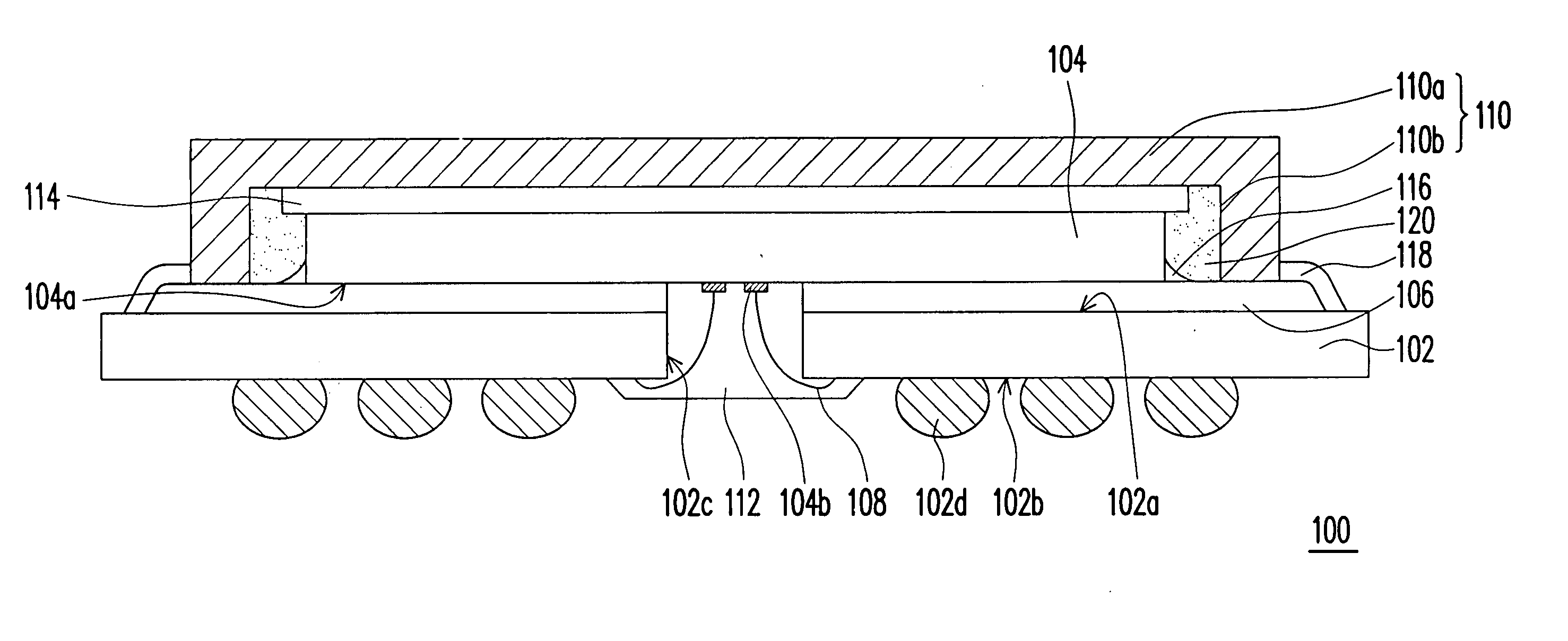
[0037]FIG. 3 is a sectional view of a chip package structure according to the present invention. Please refer to FIG. 3. The chip package structure 100 mainly comprises a substrate 102, a chip 104, a first B-stage adhesive 106, a plurality of bonding wires 108, a heat sink 110, a heat dissipation adhesive layer 114, and a molding compound 112. The substrate 102 comprises a first surface 102a, a second surface 102b and a through hole 102c. The second surface 102b is opposite to the first surface 102a while the through hole 102c connects the first surface 102a and the second surface 102b. In this embodiment, the substrate 102 is a printed circuit board such as FR-4, FR-5, BT and the like. The second surface 102b of the substrate 102 is formed with a circuit pattern (not shown) and solder balls 102d. The chip package structure 100 is electrically connected to other electronic devices (not shown) through the solder balls 102d. The chip 104 is arranged on the first surface 102a of the su...

second embodiment

[0040]FIG. 4 is a sectional view of a chip package structure according to the present invention. The chip package structure 100′ is similar to the chip package structure 100 shown in FIG. 3, and the only difference is that the supporting part 110b′ shown in FIG. 4 is inclined, such that an acute angle θ is formed between the supporting part 110b′ and the substrate 102. However, the heat sink 110 may have various types and the shape of the heat sink 110 is not limited in the present invention. Similarly, the space formed between the first B-stage adhesive 106, the chip 104 and the heat sink 110 is optionally filled with a thermal paste 120 in order to further conduct the heat generated from the chip 104 during operation.

[0041] The method of forming the chip package structures 100 and 100′ shown in FIGS. 3˜4 is illustrated in the following. When using a B-stage adhesive film as the heat dissipation adhesive layer 114, the B-stage adhesive film is attached to the heat sink 110 first an...

third embodiment

[0042]FIG. 5 is a sectional view of a chip package structure according to the present invention. The chip package structure 100″ is similar to the chip package structure 100 shown in FIG. 3, and the only difference is that the edge of the heat dissipation adhesive layer 114a formed of the B-stage adhesive or a film is aligned with that of the chip 104. The method of bonding the chip 104 and the heat sink 110 comprises the following steps. First, a thermosetting mixture is coated on the back of a wafer and then a pre-curing process is performed to form the B-stage adhesive. Next, the wafer is divided into a plurality of chips. Therefore, the edge of the B-stage adhesive is aligned with that of the chip 104. Finally, the chip 104 with the B-stage adhesive is attached to the heat sink 110.


PUM


Abstract

A chip package structure includes a substrate, a chip, a first B-stage adhesive, bonding wires, a heat sink and a molding compound. The substrate comprises a first surface, a second surface and a through hole. The chip is arranged on the first surface of the substrate and electrically connected thereto while the through hole of the substrate exposes a portion of the chip. The first B-stage adhesive is arranged between the chip and the first surface of the substrate, and the chip is attached to the substrate through the first B-stage adhesive. The bonding wires are connected between the chip exposed by the through hole and second surface of the substrate. The heat sink is arranged on the first surface of the substrate, covering the chip. The molding compound is arranged on the second surface of the substrate, covering a portion of the substrate and bonding wires.

Description

BACKGROUND OF THE INVENTION [0001] 1. Field of the Invention [0002] The present invention generally relates to a semiconductor package structure. More particularly, the present invention relates to a substrate on chip (SOC) package structure. [0003] 2. Description of Related Art [0004] The so-called “SOC (Substrate-On-Chip) packaging” refers to a common semiconductor packaging structure. In such structure, semiconductor chips are attached on a substrate with holes, and a plurality of metal bonding wires connect the substrate with the chips via the holes. Normally the substrate is also formed with a plurality of solder balls in a grid array. In the U.S. Pat. No. 6,190,943 entitled “CHIP SCALE PACKAGING METHOD”, a chip scale package structure and a packaging method are disclosed. As shown in FIG. 1, the chip scale package 20 comprises a wiring substrate 22, a semiconductor chip 24, and a plurality of spherical bonding balls 44. The substrate 22 has an upper surface 30 for attaching th...

Claims


Application Information

Patent Timeline
IPC IPC(8): H01L23/48H01L23/52H01L29/40
CPCH01L23/13H01L23/3114H01L2224/73215H01L2224/32225H01L2924/01087H01L24/48H01L2924/16152H01L2924/15311H01L2924/14H01L2224/73253H01L2224/4824H01L2224/48091H01L23/36H01L2924/00014H01L2924/00012H01L2224/451H01L2924/00H01L2224/45099H01L2224/05599
Inventor LIN, CHUN-HUNGSHEN, GENG-SHIN
Owner CHIPMOS TECH INC
Why Eureka
Try Eureka