Liquid crystal display device

a display device and liquid crystal technology, applied in the field of liquid crystal display devices, can solve the problems of increasing wasteful power consumption, poor visibility in dark places such as room interiors, and battery depletion early, and achieve the effects of accurate control of illuminating means, small fluctuation in the output of photosensors, and increased fabrication time and work

Active Publication Date: 2007-03-01
JAPAN DISPLAY WEST
View PDF14 Cites 56 Cited by
  • Summary
  • Abstract
  • Description
  • Claims
  • Application Information

AI Technical Summary

Benefits of technology

[0053] If the second mode described above is equipped a completely shielded photosensor and an unshielded photosensor for its photosensor, then the dark standard output will be stabilized by the output of the completely shielded photosensor, with the result that fluctuation in the photosensor's output will be small, as will variation in the photosensor's characteristics in the event of ambient temperature variation. Hence, it will be possible accurately to control the illuminating means to switch on and off automatically at a particular predetermined brightness.
[0054] In the second mode described above, the thin film transistor serving as, the photosensor can be fabricated simultaneously with fabrication of the thin film transistors serving as the active matrix substrate's switching elements, so that there will be no need for increased fabrication time and work in order to provide the photosensor.
[0055] If the second mode described above is configured so that the fixed-length frame periods last for an integer multiple of the vertical scan period in the drive signal for the liquid crystal display panel, and the capacitor is charged by supplying to the light sensing component a particular standard voltage whose polarity is varied with such periods, then AC component voltage will be applied to the liquid crystal layer of the liquid crystal display panel when the light sensing component is activated and it will no longer be the case that DC component voltage is always applied to such layer. As a result, deterioration of the liquid crystals can be prevented and noise will be lessened.
[0056] If in the second mode described above, the standard voltage applied to the capacitor is made negative relative to the common electrode voltage when the common electrode voltage is high level, and is made positive relative to the common electrode voltage when the common electrode voltage is low level, then AC component voltage will be applied to the liquid crystal layer of the liquid crystal display panel when the light sensing component is activated and it will no longer be the case that DC component voltage is always applied to such layer. As a result, deterioration of the liquid crystals can be prevented.
[0057] If in the second mode described above, the standard voltage is made a voltage that is intermediate between the high level and low level voltages applied to the common electrode, it will be possible to produce the standard voltage with ease.
[0058] If the second mode described above is equipped with a control means having a threshold memorizer and a comparison component in the light sensing component, and in the regular mode, in which regular light sensing is performed, the comparison component is used to compare the output of the light sensing component against the threshold value stored in the threshold memorizer so as to implement on / off control of the illumining means, while in the initial setting mode, in which the threshold value to be stored in the threshold memorizer is set, light serving as a standard is shone at the photosensor and the resulting output of the photosensor is stored in the threshold memorizer, then any fluctuation that may occur in the photosensor's characteristics will be corrected via such shining of standard light during the initial setting mode, and hence it will be possible accurately to control the illuminating means to switch on and off automatically at a particular predetermined brightness. What is more, since the end user will be able to select the standard light as desired, the end user will be able to set the backlight, etc., to turn on and off automatically at any desired ambient brightness.

Problems solved by technology

However, reflective liquid crystal display devices take the external light as their light source and consequently are poorly visible in dark places such as room interiors.
There is also the prominent problem that in some cases the backlight, etc., or frontlight will be lit unnecessarily when the external light is of ample brightness, which will increase wasteful power consumption so that in mobile equipment such as mobile telephones the battery will become depleted early.

Method used


Image

  • Liquid crystal display device
  • Liquid crystal display device
  • Liquid crystal display device

Examples


embodiment 1

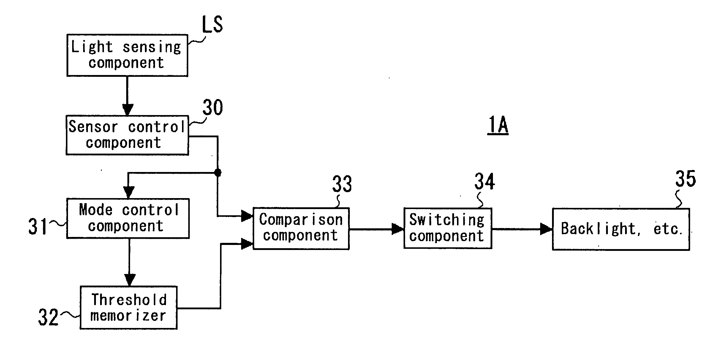
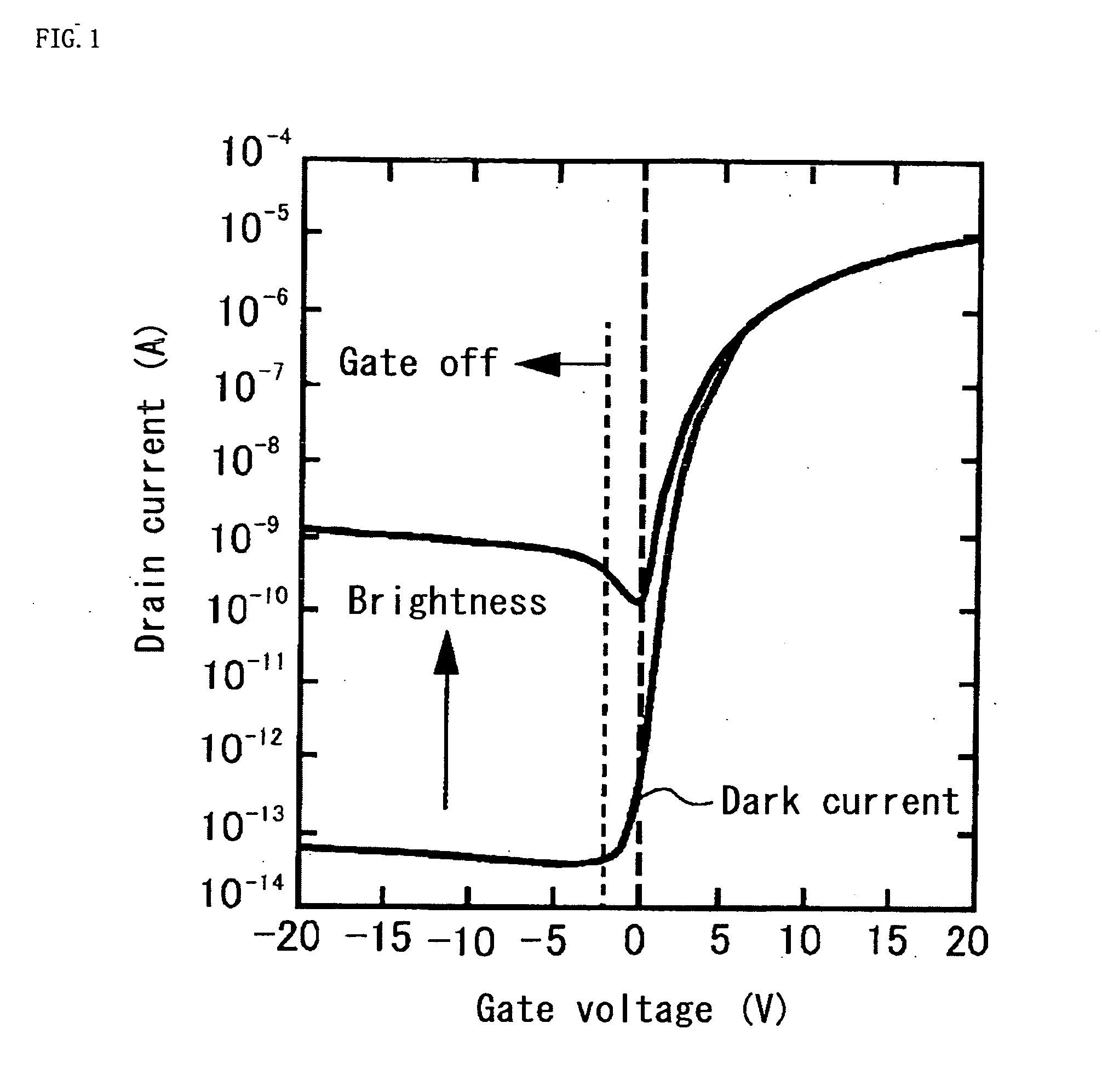
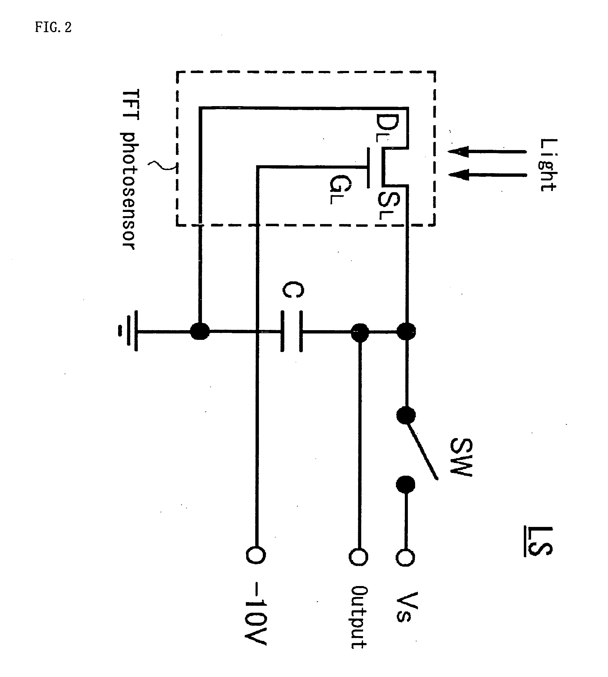
[0075] A semi-transmissive liquid crystal display device, incorporating a photosensor, of a first embodiment of the present invention will now be described with reference to FIGS. 4 and 5. FIG. 4 is a planar view illustrating schematically the active matrix substrate seen through the color filter substrate in the liquid crystal display device, while FIG. 5 is a cross-sectional view along line V-V in FIG. 4.

[0076] As shown in FIG. 5, a liquid crystal display device 1 has a structure whereby a liquid crystal layer 14 is formed between on the one hand an active matrix substrate (“TFT substrate” below) 2 which is composed of a transparent material with insulative properties, such as glass, and on whose surface a thin film transistor (TFT) or similar is mounted, and on the other hand a color filter substrate (“CF substrate” below) 25 on whose surface color filters or similar are formed.

[0077] In the display area DA of the TFT substrate 2, gate wires 4 and source wires 5 are formed in a...

embodiment 2

[0102] Although in the foregoing embodiment 1 the standard voltage VS charged into the capacitor C was voltage of a specific level, it is possible to vary such voltage with the frame periods. Accordingly, embodiment 2 of the present invention which will now be described is a liquid crystal display device 1′ in which two standard voltages are provided for charging of the capacitor C. The basic structure of the liquid crystal display device 1′ of embodiment 2 is the same as that shown in FIGS. 1 to 8 and FIG. 10 for embodiment 1, and differs from embodiment 1 only in the circuit configuration and the operating states of the light sensing component entailed by such circuit configuration, shown in FIG. 9. Below therefore, items that are structurally similar to those in embodiment 1 are referred to with the identical reference numerals and the foregoing descriptions concerning them are to be understood; the following description deals only with the structural differences from embodiment ...


PUM


Abstract

A liquid crystal display device 1 of the invention has a liquid crystal display panel in which a liquid crystal layer 14 is provided between a TFT substrate 2 and a CF substrate 25 that has a common electrode 26, a light sensing component LS1 with a TFT photosensor that senses external light, and an illuminating means controlled according to the output of the light sensing component. The light sensing component is deployed at the periphery of the TFT substrate's display area DA and uses a thin film transistor as photosensor. A capacitor C is connected between source and drain electrodes SL, DL for such TFT photosensor. One of the capacitor's terminals is connected to a standard voltage source VS via a switch element SW, and the other to the common electrode 26. Voltage that is always lower than the voltage applied to the common electrode by an amount corresponding to a reverse bias voltage is applied to the gate electrode GL for the TFT photosensor. The capacitor's voltage a certain time after the switch element turns off is output. As a result, it will be possible to provide a liquid crystal display device in which the light sensing component incorporated in the liquid crystal display panel is not susceptible to the influence of the drive signals for the display panel, and in which the light sensing component does not induce deterioration of the liquid crystals.

Description

FIELD OF THE INVENTION [0001] The present invention relates to a liquid crystal display device. More particularly, it relates to a liquid crystal display device having a backlight, frontlight or similar light source, wherein the brightness of the light source can be varied according to the brightness of the external light. BACKGROUND OF THE INVENTION [0002] Over recent years the use of liquid crystal display devices has spread rapidly not only in information and telecommunications equipment but in electrical equipment in general. Especially in mobile equipment, use is often made, in order to reduce power consumption, of the reflective type of liquid crystal display device, which does not require a backlight or sidelight as the transmissive type does. (Below, “backlight, etc.” is used to include both backlight and sidelight.) However, reflective liquid crystal display devices take the external light as their light source and consequently are poorly visible in dark places such as room...

Claims


Application Information

Patent Timeline
Patent Type & Authority Applications(United States)
IPC IPC(8): G09G3/36
CPCG02F2001/13312G09G3/3406G09G3/3648G09G2360/144G09G2300/0456G09G2320/0626G09G2300/0426G02F1/13312G02F1/133G02F1/136
Inventor SANO, YUTAKAKUNIMORI, TAKASHIYASUMORI, MASANORITANAKA, TOSHIHIKO
Owner JAPAN DISPLAY WEST
Why Eureka
Try Eureka