

Assembly for an electronic component
a technology of electronic components and components, applied in the direction of printed circuit manufacturing, printed circuit components, electrical apparatus construction details, etc., can solve the problems of poor heat removal poor thermal performance and efficiency of high-power electronic components, and inability to use parts that require good thermal performance and efficiency
- Summary
- Abstract
- Description
- Claims
- Application Information
AI Technical Summary
Benefits of technology
Problems solved by technology
Method used
Image

Examples
Embodiment Construction
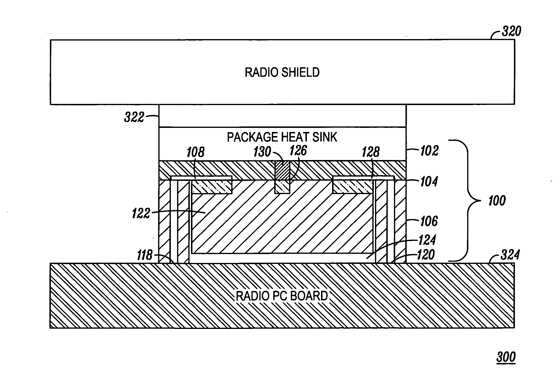
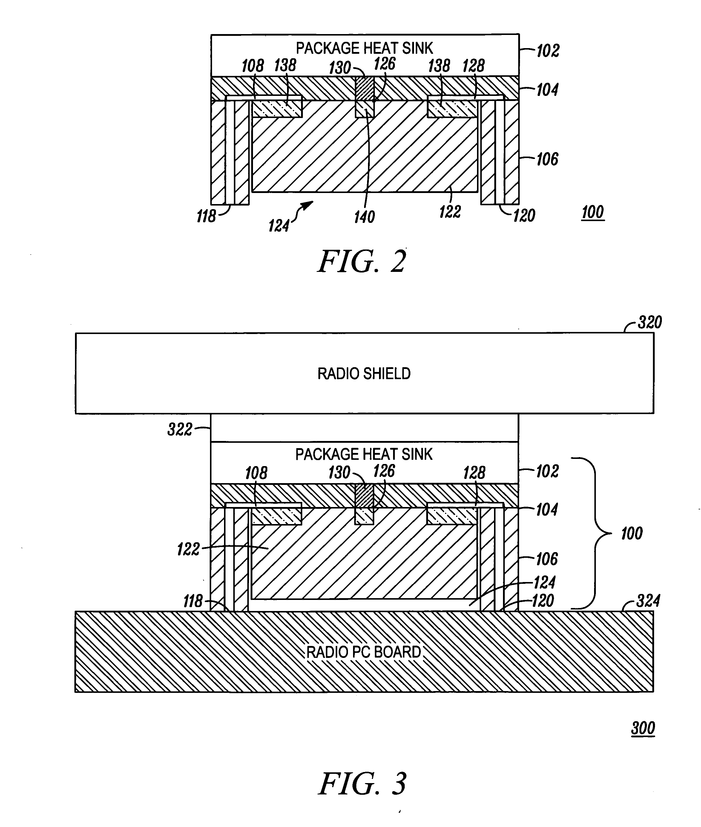
[0010] Briefly in accordance with the present invention, there is provided herein a an assembly which takes an existing packaged high power electronic component and repackages it in an assembly that allows the heat to be removed through direct chassis contact with the top of the assembly. A high power electronic component can be operated at optimum power levels without degrading performance when contained in the assembly.
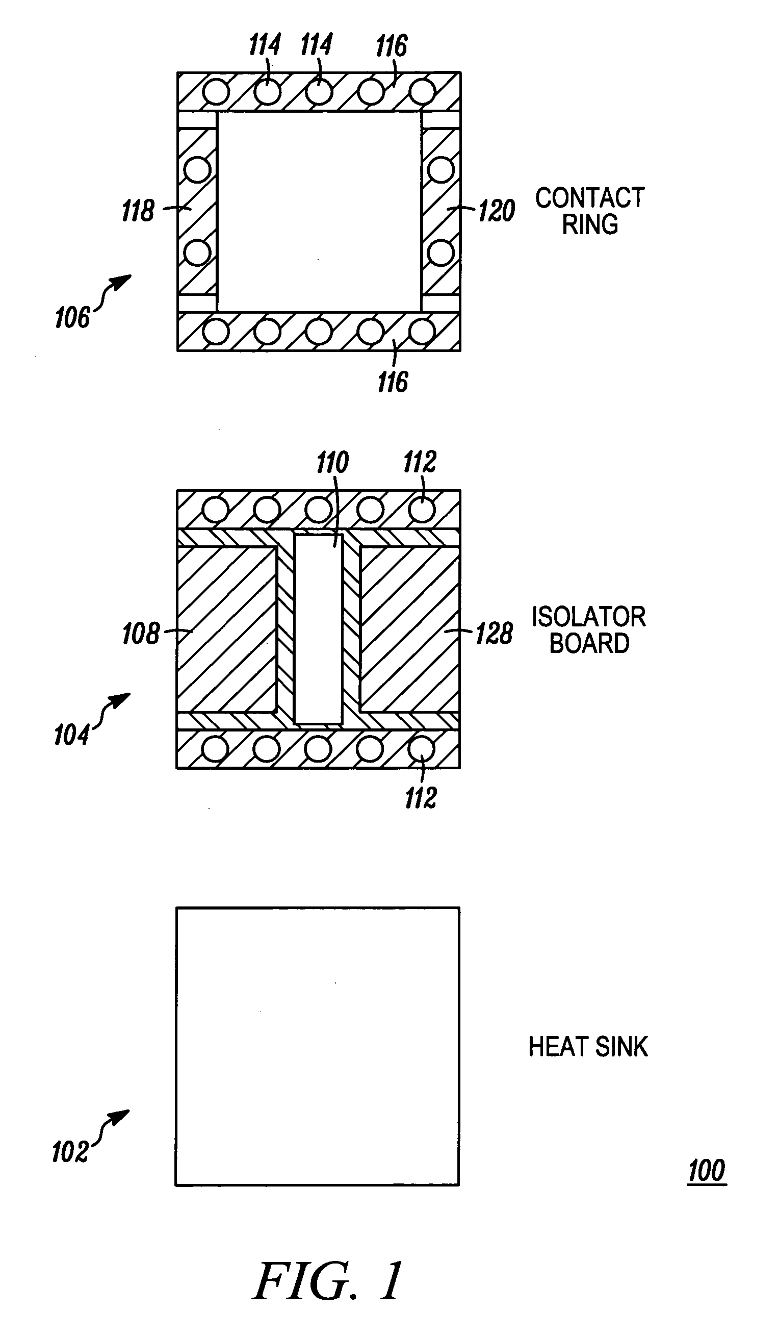
[0011]FIG. 1 shows an exploded view of three main pieces for an assembly 100 including a heat sink 102, a printed circuit board (pcb) isolator 104 and a contact ring 106 in accordance with the present invention. Printed circuit board isolator 104 includes an opening 110 through which to solder an active electronic component (shown in FIG. 2) to the heat sink 102. Printed circuit board isolator 104 also includes contact pads 108, 128 upon which to solder electronic component contacts. Via through holes 112 are formed through the pcb isolator 104 for coupling the iso...
PUM
 Abstract
Description
Claims
Application Information