Semiconductor device

a semiconductor and device technology, applied in the field of semiconductor devices, can solve problems such as the inability to obtain optimal layout systems, and achieve the effect of simplifying the layout structure of semiconductors

Inactive Publication Date: 2007-03-01
RENESAS TECH CORP
View PDF2 Cites 33 Cited by
  • Summary
  • Abstract
  • Description
  • Claims
  • Application Information

AI Technical Summary

Benefits of technology

[0008] An object of the present invention is to provide a technique capable of simplifying a layout structure of a semiconductor device having a semiconductor memory section in which an input port and an output port are separated from each other, and which includes a bypass function.
[0010] Since the first bypass line is arranged through between the first and second memory cell arrays in the layout structure in plan view, it is possible to install wiring of the first bypass line without effects of the layout structure within the region where the memory cell array is formed. This can result simplification of the layout structure, thereby allowing size reduction of the device and simplification of the device production process. Further, it is possible to reduce an effect exerted on data, transmitted through the first bypass line, by the wiring potential within the region where the memory cell array is formed.
[0012] In the layout structure where the memory cell array is arranged between the input buffer circuit and the output buffer circuit, it is possible to simplify the layout structure since the bypass line, the write bit line, the read bit line, the power wiring and the ground wiring are arranged on a region where the plurality of memory cells are formed in the memory cell array. This can result in size reduction of the device and simplification of the device production process.
[0014] Extension of the write bit line from the memory cell array to the output buffer circuit enables output of data, having been inputted into the input port, as it is to the output port. In this manner, the bypass function is realized by use of the write bit line, thereby allowing simplification of the layout structure. This can result in size reduction of the device and simplification of the device production process.
[0016] Extension of the read bit line from the memory cell array to the input buffer circuit enables output of data, having been inputted into the input port, as it is to the output port. In this manner, the bypass function is realized by use of the read bit line, thereby allowing simplification of the layout structure. This can result in size reduction of the device and simplification of the device production process.

Problems solved by technology

It is therefore not possible to obtain an optimum layout system from the technique of Japanese Patent Application Laid-Open No. 09-54142 (1997).

Method used


Image

  • Semiconductor device
  • Semiconductor device
  • Semiconductor device

Examples


first embodiment

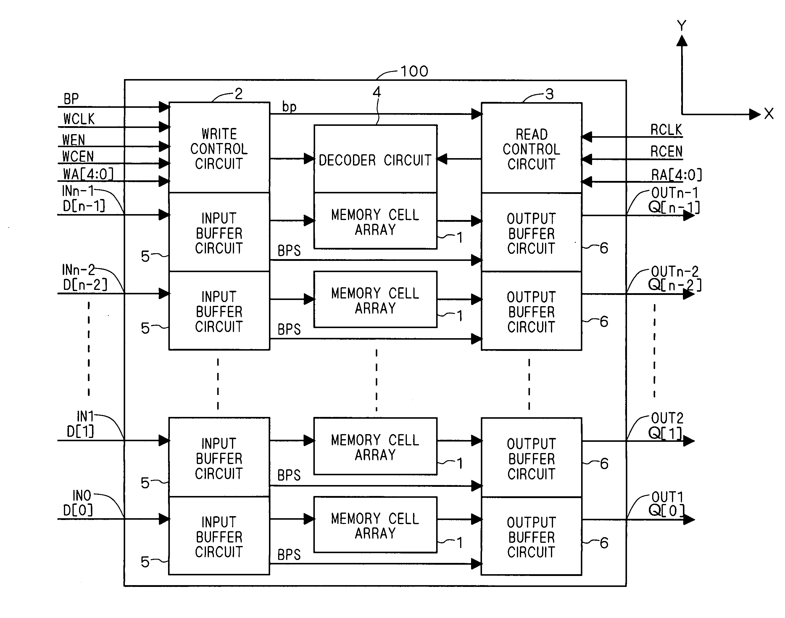
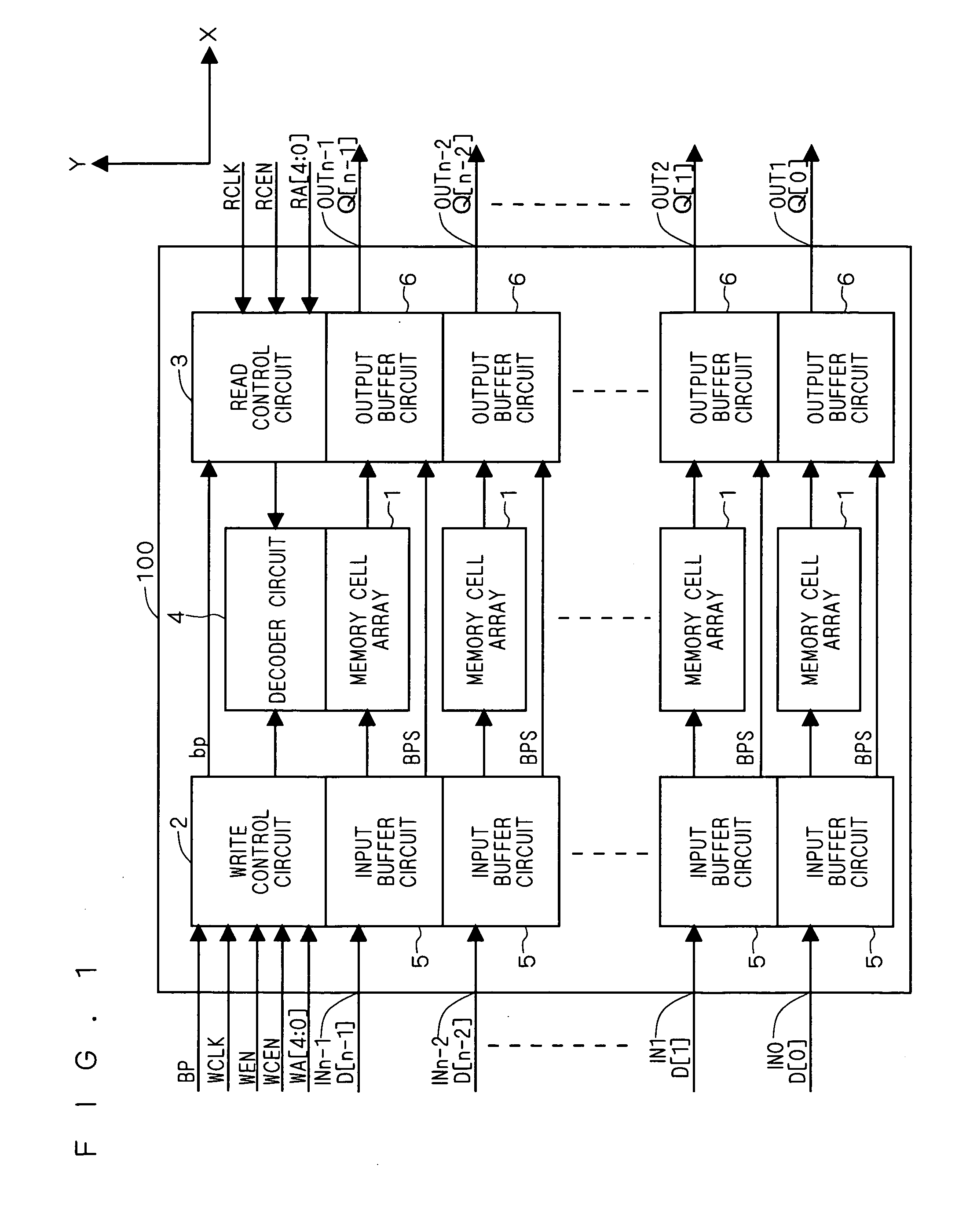
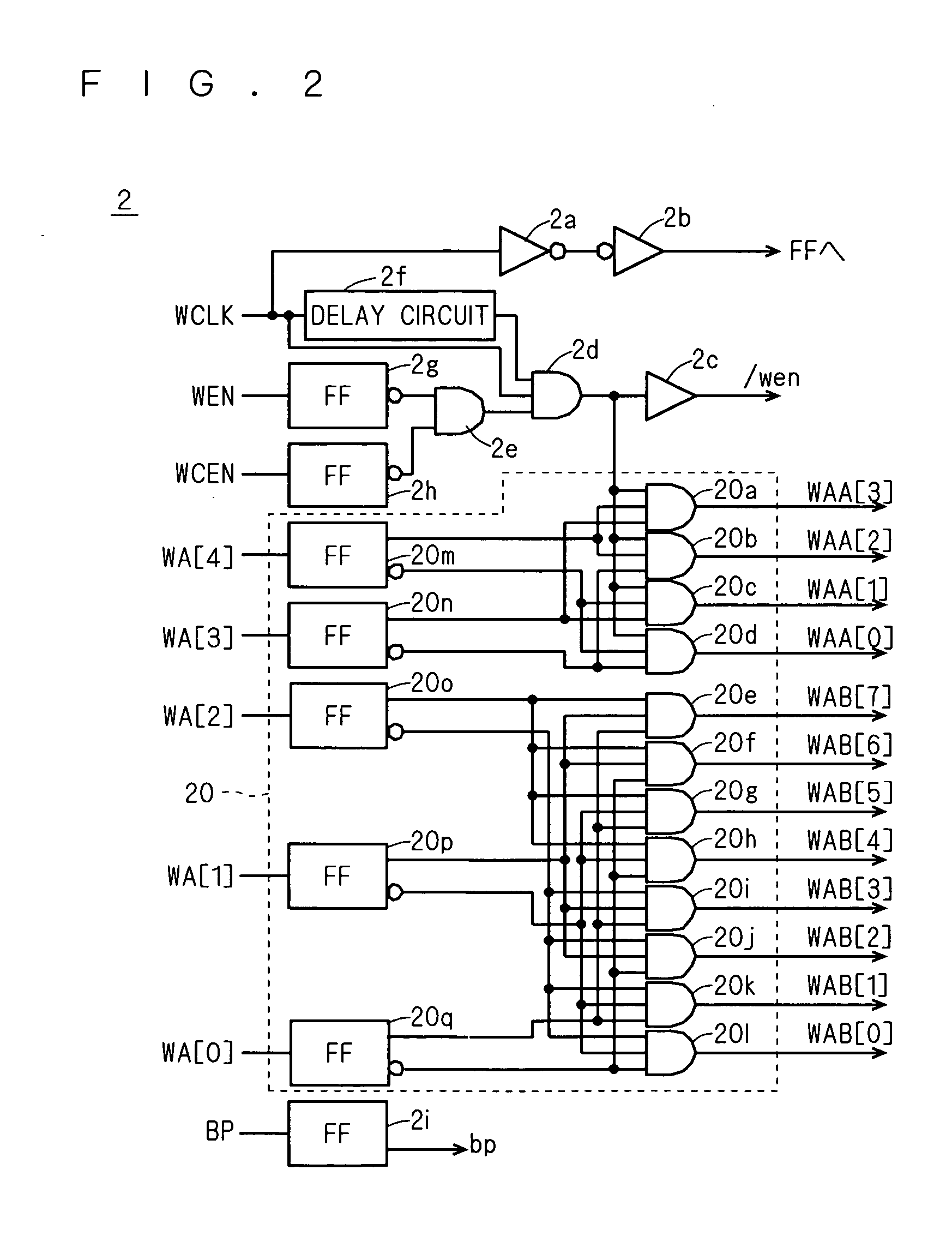
[0037]FIG. 1 is a plan view schematically showing a layout structure of a semiconductor memory device 100 according to a first embodiment of the present invention. As shown in FIG. 1, the semiconductor memory device 100 according to the first embodiment includes: n input ports (n≧1) IN0 to INn-1; n output ports OUT0 to OUTn-1; a write control circuit 2; a read control circuit 3; and a decoder circuit 4. Further, the semiconductor memory device according to the first embodiment is provided with n groups each consisting of one memory cell array 1, one input buffer circuit 5 and one output buffer circuit 6.

[0038] n-bit input data D[n-1:0] is inputted into the semiconductor memory device 100, and n-bit output data Q[n-1:0] is outputted from the semiconductor memory device 100. Input data D[0] to D[n-1] are respectively inputted into the input ports IN0 to INn-1, and output data Q[0] to Q[n-1] are respectively outputted from the output ports OUT0 to OUTn-1.

[0039] Input data D[i] among ...

second embodiment

[0091]FIG. 10 is a plan view schematically showing a layout structure of the semiconductor memory device 110 according to a second embodiment. The semiconductor memory device 110 according to the second embodiment is a device that can realize the bypass function without arrangement of the bypass line BPL for intended for the purpose by arranging, in the aforesaid semiconductor memory device 100 of the first embodiment, a write control circuit 12 in place of the write control circuit 2, n input buffer circuits 15 in place of the n input buffer circuits 5, and n output buffer circuits 16 in place of the output buffer circuits 6. As in the first embodiment, one input buffer circuit 15, one output buffer circuit 16 and one memory cell array 1 constitute one group. The layout of the write control circuit 12, the input buffer circuit 15 and the output buffer circuit 16 is the same as the layout of the write control circuit 2, the input buffer circuit 5 and the output buffer circuit 6 acco...

third embodiment

[0108] FIGS. 13 to 16 are plan views schematically showing a circuit configuration of a semiconductor memory device according to a third embodiment of the present invention. The semiconductor memory device according to the third embodiment is a device formed by arranging, in the semiconductor memory device 110 according to the second embodiment, n memory cell arrays 21 in place of the n memory cell arrays 1, a write control circuit 22 in place of the write control circuit 12, a read control circuit 33 in place of the read control circuit 3, a decoder circuit 24 in place of the decoder circuit 4, n input buffer circuits 25 in place of the n input buffer circuits 15, and n output buffer circuits 26 in place of the output buffer circuits 16. As in the second embodiment, one input buffer circuit 25, one output buffer circuit 26 and one memory cell array 1 constitute one group. The layout of the memory cell array 21, the write control circuit 22, the read control circuit 23, the decoder ...


PUM


Abstract

The present invention provides a technique capable of simplifying a layout structure of a semiconductor device having a semiconductor memory section in which an input port and an output port are separated from each other, and which includes a bypass function. In a semiconductor memory device to be used as a semiconductor memory section of the semiconductor device, in a bypass mode, an output buffer outputs input data transmitted through a bypass line, extending from an input buffer circuit to the output buffer circuit, to an output port. In the layout structure of the semiconductor memory device, in plan view, a memory cell array is arranged between the input buffer circuit and the output buffer circuit, and a bypass line is arranged through between the memory cell arrays.

Description

BACKGROUND OF THE INVENTION [0001] 1. Field of the Invention [0002] The present invention relates to a semiconductor device including a semiconductor memory section with its input port and output port separated from each other. [0003] 2. Description of the Background Art [0004] There have hitherto been proposed a variety of techniques regarding a multi-port memory with its input port and output port separated from each other. For example, Japanese Patent Application Laid-Open No. 09-54142 (1997) discloses a technique of arranging a bypass means of outputting data, having been inputted into an input port, directly to an output port to perform a test on a semiconductor memory device by use of the bypass means. [0005] Further, other techniques regarding a semiconductor memory device are described in Japanese Patent Application Laid-Open Nos. 2001-23400 and 05-74198 (1993). [0006] As in the technique described in Japanese Patent Application Laid-Open No. 09-54142 (1997), when the bypass...

Claims


Application Information

Patent Timeline
Patent Type & Authority Applications(United States)
IPC IPC(8): G11C5/02
CPCG11C7/1006G11C2207/108G11C11/412G11C8/16G11C7/10G11C7/18G11C8/14
Inventor MIYANISHI, ATSUSHI
Owner RENESAS TECH CORP
Why Eureka
Try Eureka