Printing plate, method of fabricating the same, and method of fabricating flat panel display using the same

a printing plate and flat panel technology, applied in the field of printing plates, can solve the problems of affecting the production efficiency of the product, affecting the quality of the product, and affecting the quality of the product, and achieve the effect of high precision and high precision

Active Publication Date: 2007-03-01
LG DISPLAY CO LTD
View PDF4 Cites 9 Cited by
  • Summary
  • Abstract
  • Description
  • Claims
  • Application Information

AI Technical Summary

Benefits of technology

[0012] An objective of the present invention is to provide a printing plate and a method of fabricating the same, capable of forming fine patterns having a high precision.
[0013] Another objective of the present invention is to provide a method of fabricating a flat panel display with fine patterns having a high precision.

Problems solved by technology

In the photolithography process, however, complex processes such as an exposure process and a development process are performed, thus degrading the production efficiency.
Unlike the photolithography process, the printing method has an excellent advantage in terms of production efficiency, but it has a disadvantage in forming a fine pattern.
For example, in the case of a screen printing method, since a resist pattern has a thickness of several ten micrometers, it can form a resist pattern with an excellent corrosion resistance, but it is difficult to form a complicated and fine pattern.
However, it is difficult to form a printing plate with a fine recessed pattern.
At this point, if the recessed pattern is formed to have a small depth so as to decrease the width of the recessed pattern, the thickness of the resist pattern becomes small, resulting in a decrease in the corrosion resistance.
Therefore, when the interconnections are formed by patterning the conductive layer, it is practically impossible to form the interconnections in a desired pattern.

Method used


Image

  • Printing plate, method of fabricating the same, and method of fabricating flat panel display using the same
  • Printing plate, method of fabricating the same, and method of fabricating flat panel display using the same
  • Printing plate, method of fabricating the same, and method of fabricating flat panel display using the same

Examples


Embodiment Construction

[0024] Reference will now be made in detail to the preferred embodiments of the present invention, examples of which are illustrated in the accompanying drawings. Wherever possible, the same reference numbers will be used throughout the drawings to refer to the same or like parts.

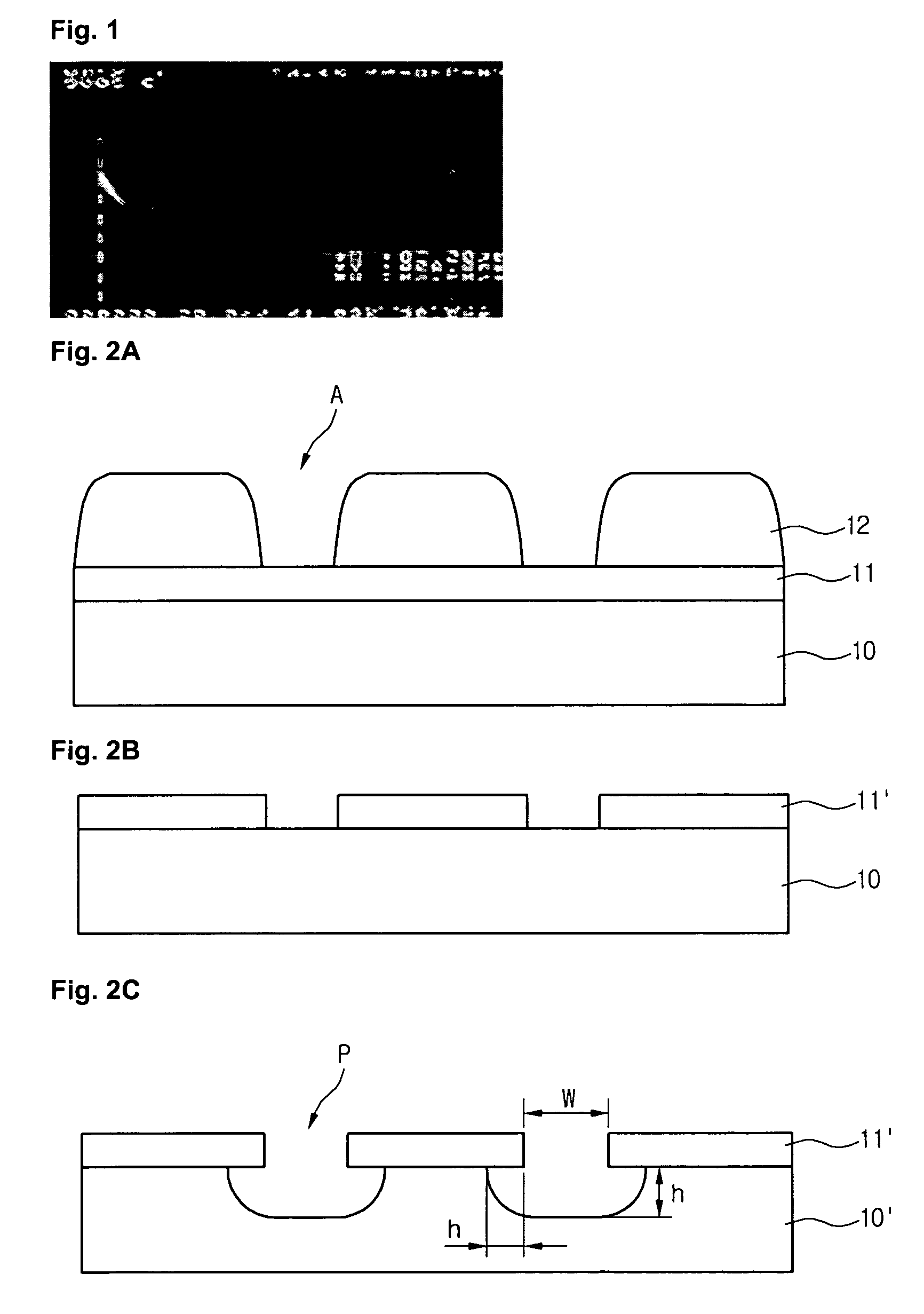
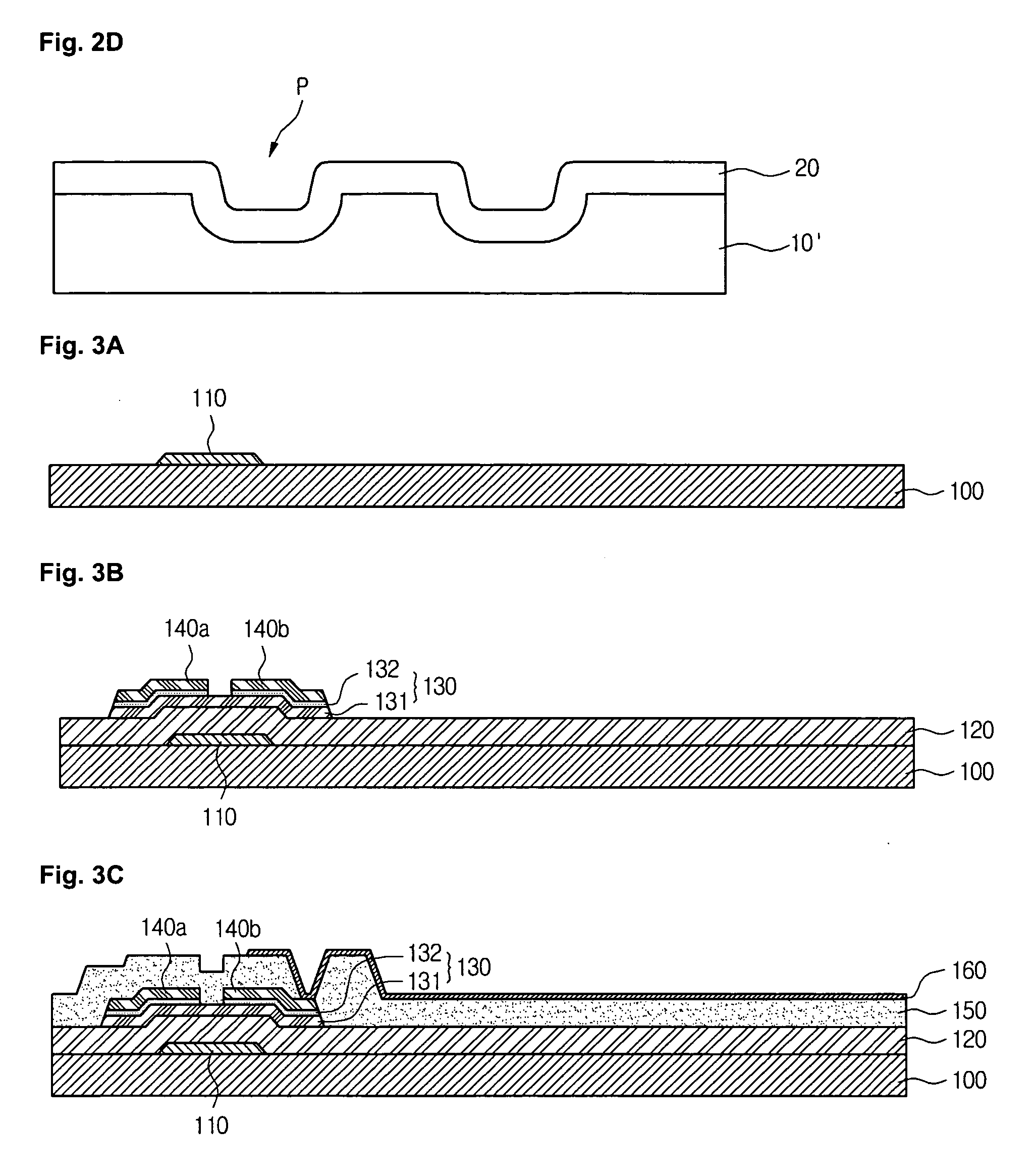
[0025]FIGS. 2A to 2D are sectional views for explaining a printing plate and a method of fabricating the same according to an embodiment of the present invention.

[0026] Referring to FIG. 2A, a substrate 10 is prepared. The substrate 10 may be formed of material selected from the group consisting of glass, plastic, and metal. A metal layer 11 is deposited on the substrate 10. It is preferable that the metal layer 11 should have a resistance against an etchant. The reason for this is that the metal layer 11 will be used as a mask in forming a recessed pattern, which will be described later.

[0027] A resist layer is formed on the metal layer 11 by a typical method and is exposed and developed to form resist...


PUM

PropertyMeasurementUnit
thicknessaaaaaaaaaa
poweraaaaaaaaaa
conductiveaaaaaaaaaa

Abstract

A method of fabricating a printing plate includes: preparing a substrate; forming a metal layer on an entire surface of the substrate; forming a resist pattern on the metal layer, the resist pattern having a fine pattern exposing a portion of the metal layer; wet etching the exposed metal layer, and removing the resist pattern to form a metal layer pattern exposing a portion of the substrate; wet etching the exposed substrate, and removing the metal layer pattern to form a recessed pattern; and forming a compensation layer on an entire surface of the substrate where the recessed pattern is formed.

Description

FIELD OF THE INVENTION [0001] The present invention relates to a method of fabricating a flat panel display, and more particularly, to a printing plate, a method of fabricating the same, and a method of fabricating a flat panel display using the same, capable of forming fine patterns. BACKGROUND OF THE INVENTION [0002] With the rapid development of the information society, flat panel displays with favorable characteristics, such as slim profile, lightweight, and low power consumption are increasingly demanded. In addition, fineness and high preciseness are required in interconnections among components of the flat panel device. [0003] Related art interconnections are formed by forming resist patterns using a photolithography or printing method and patterning a conductive layer along the resist patterns. When forming the fine interconnections, it is important to finely form the resist patterns. [0004] At this point, the photolithography process is advantageous to forming the fine resi...

Claims


Application Information

Patent Timeline
Patent Type & Authority Applications(United States)
IPC IPC(8): G03F7/00B41C1/00B41F17/14B41N1/06B41N1/12G03F7/20H01L51/50H05B33/10
CPCB41C1/00H05K2203/0537B41N1/006B41N1/04B41N1/06B82Y10/00B82Y40/00G03F7/0002H01L27/1214H01L27/3244H01L51/0004H01L51/56H05K3/0079H05K3/1275H05K2203/0143H05K2203/0534B41M3/003H01L27/1288H10K59/12H10K71/13H10K71/00G02F1/1333
Inventor YOO, SOON SUNGCHANG, YOUN GYOUNGCHO, HEUNG LYUL
Owner LG DISPLAY CO LTD
Why Eureka
Try Eureka