Transistor gate forming methods and transistor structures

a technology of transistors and transistors, applied in the direction of basic electric elements, electrical equipment, semiconductor devices, etc., can solve the problems of difficulty in substituting metal gate electrode materials for polysilicon, polysilicon exhibits a generalized too high resistivity for aggressive device scaling,

Active Publication Date: 2007-03-01
MICRON TECH INC
View PDF48 Cites 40 Cited by
  • Summary
  • Abstract
  • Description
  • Claims
  • Application Information

AI Technical Summary

Benefits of technology

[0005] In a further aspect of the invention, a transistor structure includes a gate line opening extending into a semiconductive substrate, the opening having a semiconductive bottom and semiconductive side walls. A gate dielectric layer is within the opening over the semiconductive side walls and semiconductive bottom, the dielectric layer having an insulative bottom and insulative side walls. A gate metal lay

Problems solved by technology

However, polysilicon exhibits a resistivity generally considered too high for aggressive device scaling.
While metal gate electrode materials appear to function effectively in simple configura

Method used


Image

  • Transistor gate forming methods and transistor structures
  • Transistor gate forming methods and transistor structures
  • Transistor gate forming methods and transistor structures

Examples


example

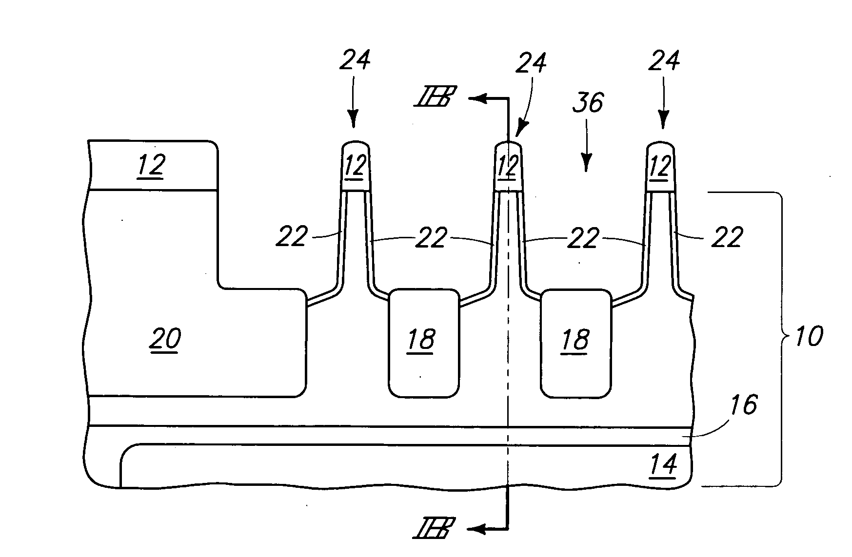
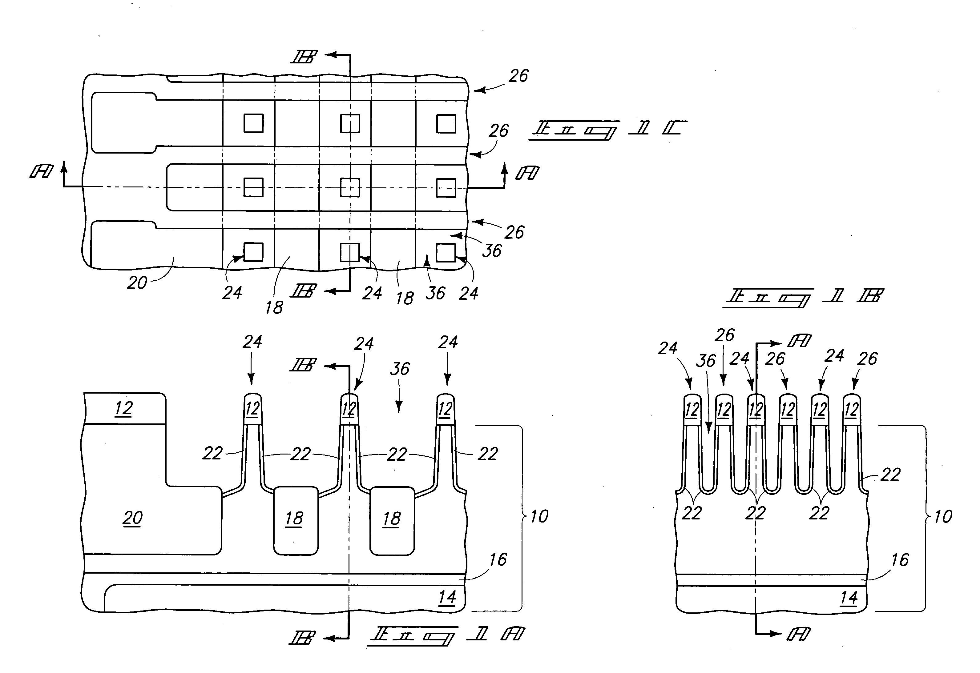
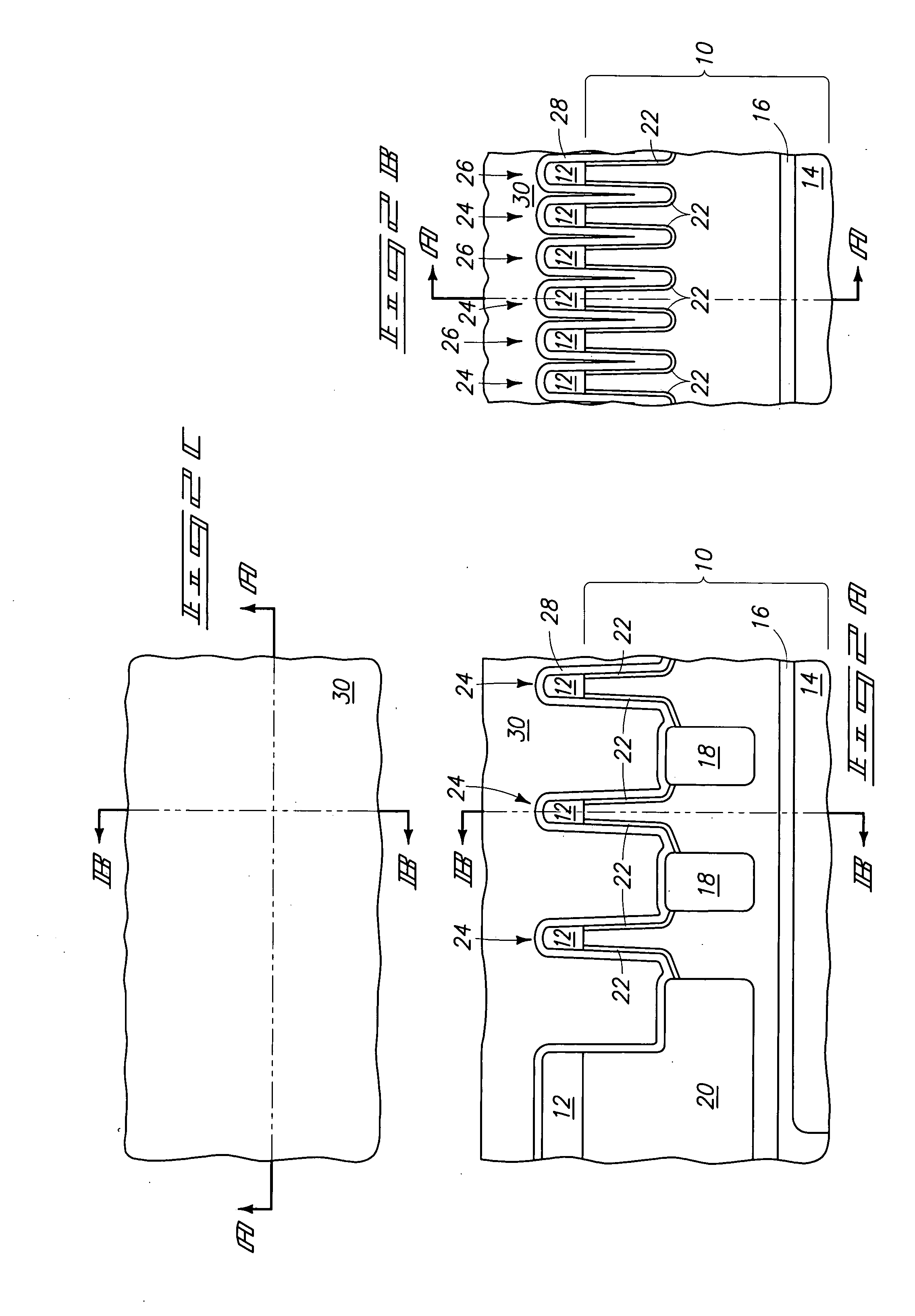
[0044] A transistor structure as shown in FIGS. 5A-C was formed by supercritical fluid deposition of 150 Angstroms of TiN on the structure shown in FIGS. 1A-C. 500 to 2,000 Angstroms of polysilicon with a resistivity of 20 to 200 Ohm-centimeter were formed on the TiN by CVD. Chemical mechanical polishing followed, removing polysilicon and stopping on Si3N4 masking layer 12. Polysilicon was recessed into line openings 36 using 116 sec. of RIE in a LAM 9400 with 80 to 150 sccm of HBr and 100 to 200 sccm of He at a pressure of 50 to 100 milliTorr and a power of 125 to 225 Watts. Wet etching at 55° C. using 2 volume % NH4OH and 3 volume % H2O2 in deionized water for 7 min. produced the FIGS. 5A-C structure. Scanning electron microscopy of cross-sections and tilted top views did not reveal any cracks or stringers. The processing was repeated several times within the described parameter ranges, producing highly similar results. Subsequent Rs testing revealed a range of 28.9 to 32.3 Ohm / sq...


PUM


Abstract

A transistor gate forming method includes forming a metal layer within a line opening and forming a fill layer within the opening over the metal layer. The fill layer is substantially selectively etchable with respect to the metal layer. A transistor structure includes a line opening, a dielectric layer within the opening, a metal layer over the dielectric layer within the opening, and a fill layer over the metal layer within the opening. The metal layer/fill layer combination exhibits less intrinsic less than would otherwise exist if the fill layer were replaced by an increased thickness of the metal layer. The inventions apply at least to 3-D transistor structures.

Description

TECHNICAL FIELD [0001] The invention pertains to transistor gate forming methods and transistor structures. BACKGROUND OF THE INVENTION [0002] A continuing interest exists in aggressively reducing feature sizes of integrated circuitry. In conventional semiconductor-based integrated circuitry, polysilicon is often used as a gate electrode material in a field effect transistor (FET). However, polysilicon exhibits a resistivity generally considered too high for aggressive device scaling. Metal gate electrode materials have been identified to replace polysilicon. While metal gate electrode materials appear to function effectively in simple configurations, difficulties can arise in substituting metal gate electrode materials for polysilicon in three-dimensional (3-D) transistor devices and other devices with a more complex configuration. Accordingly, a desire exists to develop transistor gate forming methods and transistor structures capable of implementing metal gate electrode materials...

Claims


Application Information

Patent Timeline
IPC IPC(8): H01L21/336
CPCH01L29/42392H01L29/78696H01L29/66787
Inventor TANG, SANH D.HALLER, GORDON A.RAGHU, PRASHANTIYER, RAVI
Owner MICRON TECH INC
Why Eureka
Try Eureka