Methods of forming field effect transistors on substrates

a field effect transistor and substrate technology, applied in the direction of transistors, semiconductor devices, electrical equipment, etc., can solve the problems of affecting materials, affecting the performance of transistors,

Inactive Publication Date: 2007-03-01
MICRON TECH INC
View PDF62 Cites 47 Cited by
  • Summary
  • Abstract
  • Description
  • Claims
  • Application Information

AI Technical Summary

Benefits of technology

[0007] The invention includes methods of forming field effect transistors. In one implementation, the invention encompasses a method of forming a field effect transistor on a substrate, where the field effect transistor comprises a pair of conductively doped source/drain regions, a channel region received in

Problems solved by technology

This results in thinner layers and smaller geometries.
Such materials can be adversely affected by the typical temperatures and times required to achieve dopant activation by anneal.
For example, certain metal materials (i.e., titanium, titanium nitride, molybdenum s

Method used


Image

  • Methods of forming field effect transistors on substrates
  • Methods of forming field effect transistors on substrates
  • Methods of forming field effect transistors on substrates

Examples


Embodiment Construction

[0033] This disclosure of the invention is submitted in furtherance of the constitutional purposes of the U.S. Patent Laws “to promote the progress of science and useful arts” (Article 1, Section 8).

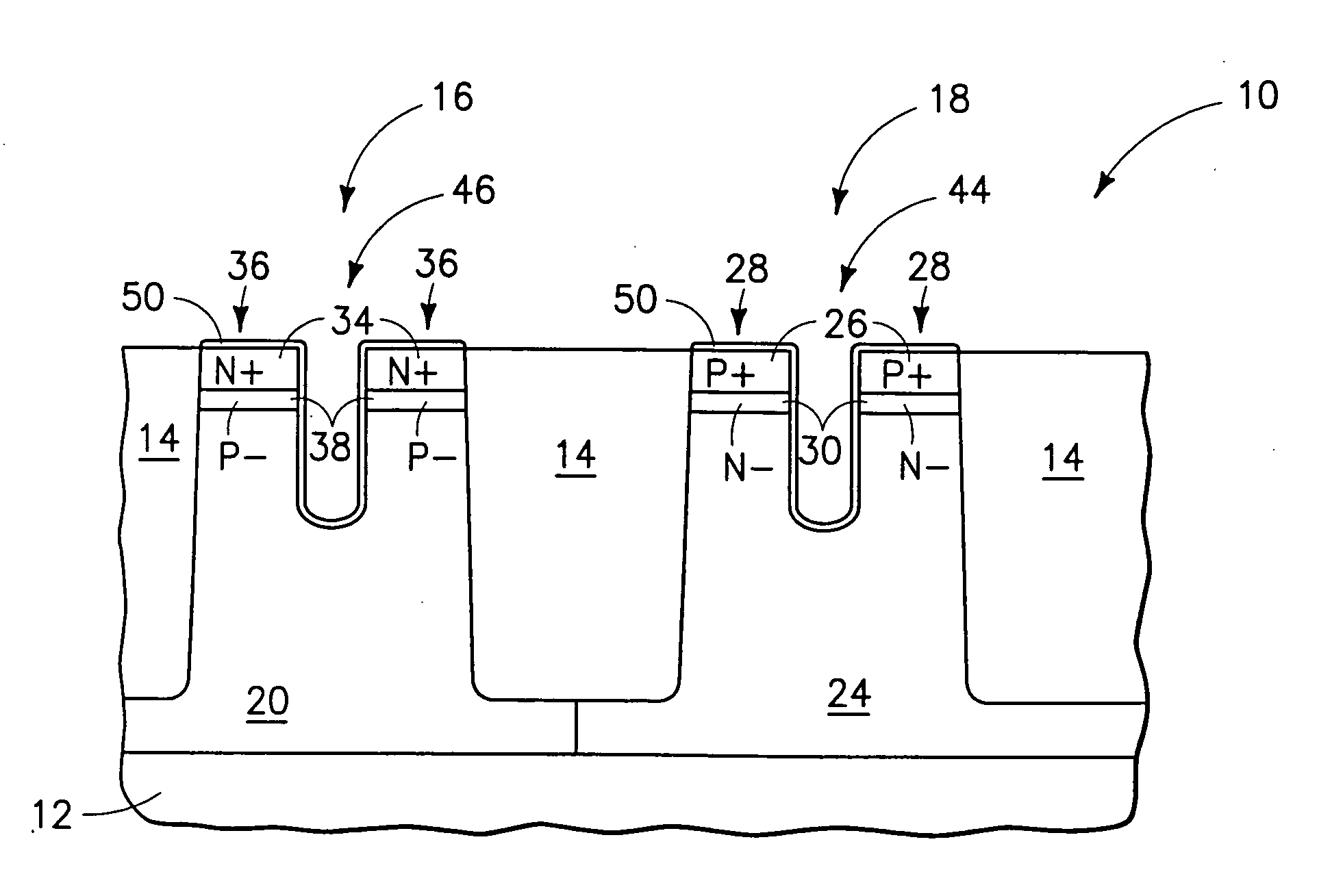
[0034] Exemplary preferred methods of forming a field effect transistor on a substrate are described with reference to FIGS. 1-20. By way of example only, the field effect transistor might be p-type or n-type. Regardless, the field effect transistor will comprise a pair of conductively doped source / drain regions, a channel region received intermediate the pair of source / drain regions, and a transistor gate received operably proximate the channel region. An exemplary preferred embodiment method is described in forming both an n-channel field effect transistor and a p-channel field effect transistor on a substrate, although methods in accordance with the invention might be utilized to fabricate only a single conductivity type field effect transistor.

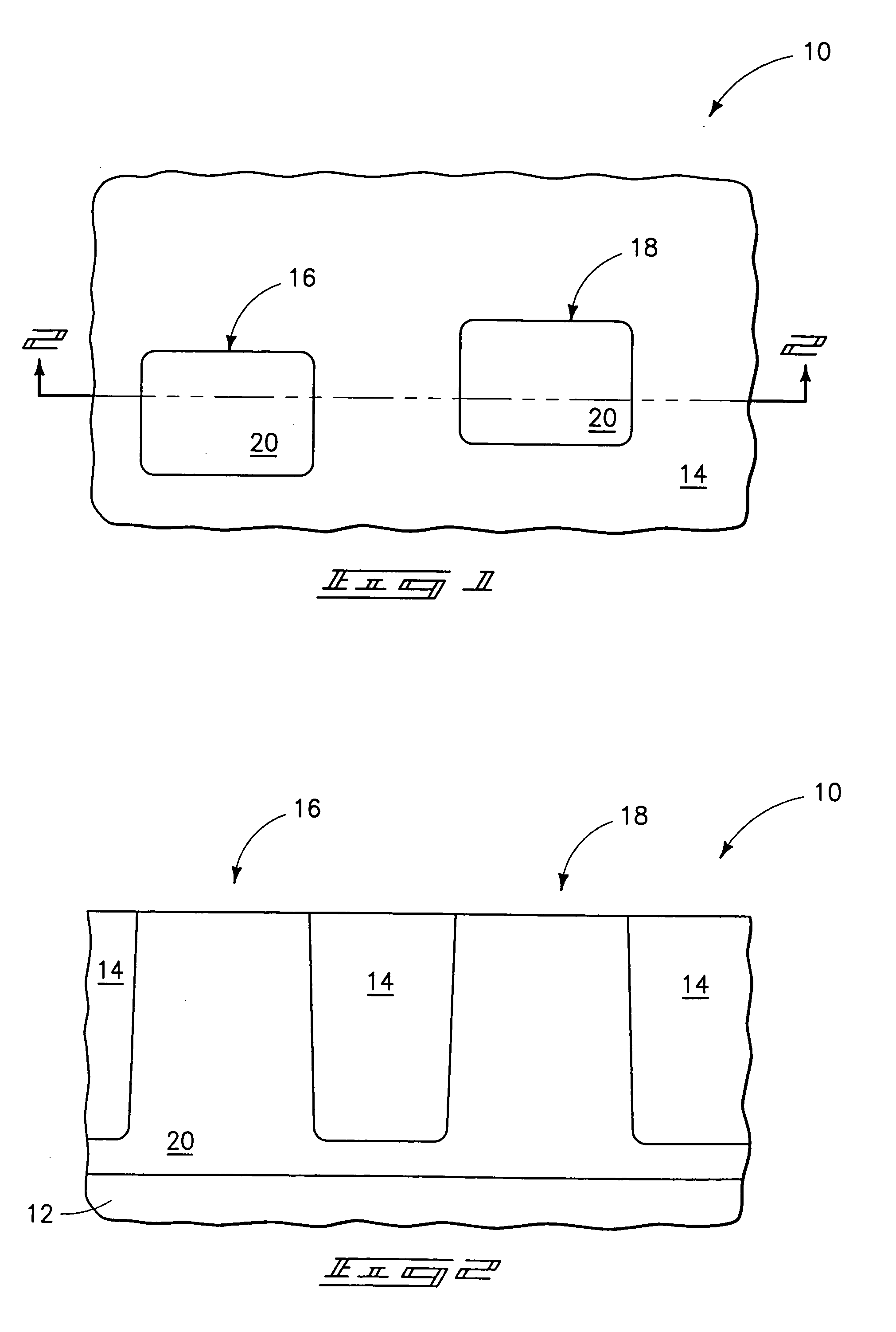
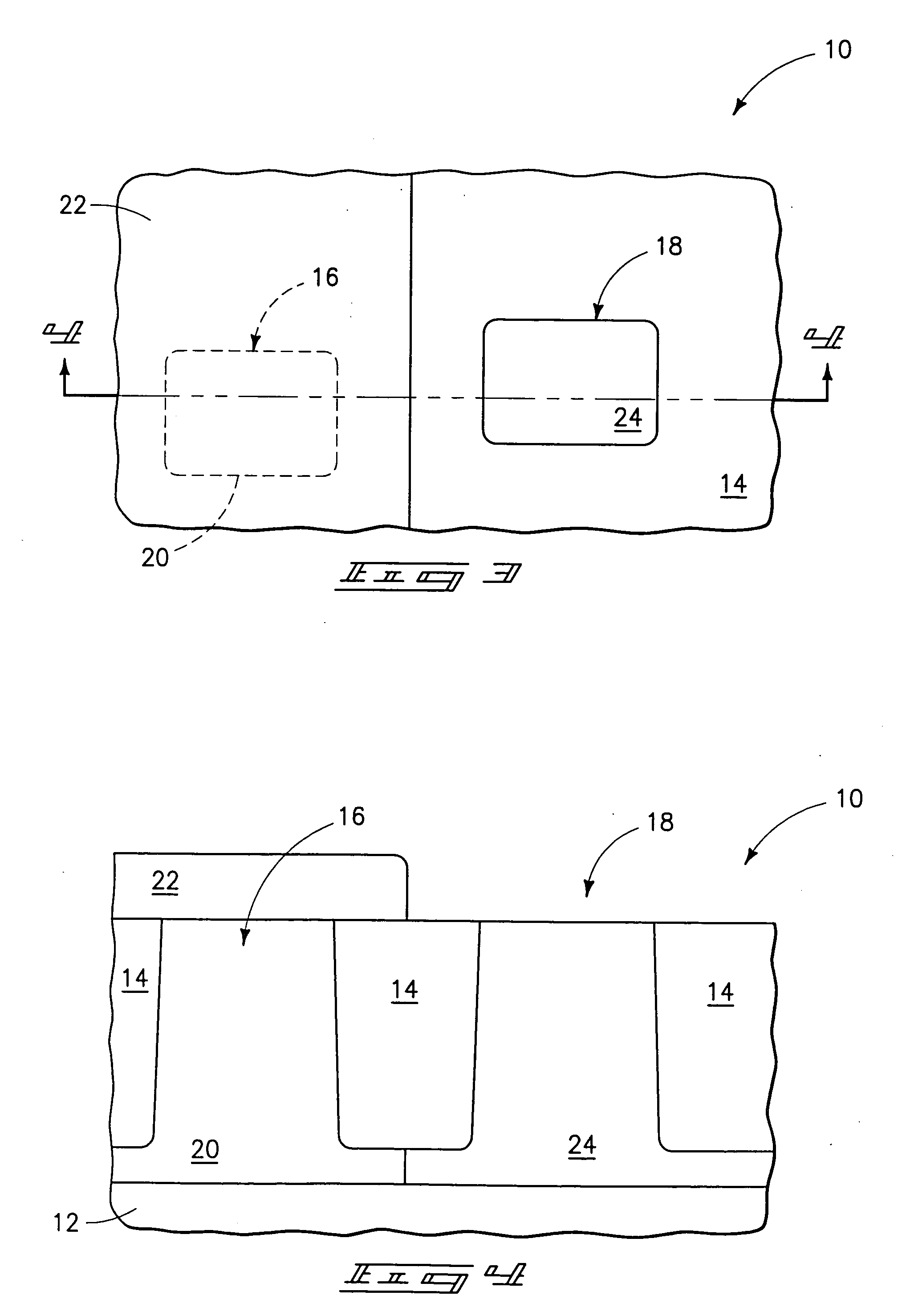
[0035] Referring to FIGS. 1 and 2, an ...


PUM


Abstract

The invention includes methods of forming field effect transistors. In one implementation, the invention encompasses a method of forming a field effect transistor on a substrate, where the field effect transistor comprises a pair of conductively doped source/drain regions, a channel region received intermediate the pair of source/drain regions, and a transistor gate received operably proximate the channel region. Such implementation includes conducting a dopant activation anneal of the pair of source/drain regions prior to depositing material from which a conductive portion of the transistor gate is made. Other aspects and implementations are contemplated.

Description

TECHNICAL FIELD [0001] This invention relates to methods of forming field effect transistors. BACKGROUND OF THE INVENTION [0002] A continuing goal in integrated circuitry design is to make ever denser, and therefore smaller, circuit devices. This results in thinner layers and smaller geometries. Further, new deposition techniques and materials are constantly being developed to enable circuit devices to be made smaller than the previous generations. Additionally, circuit design sometimes fabricates the devices to be substantially horizontally oriented relative to an underlying substrate, and sometimes substantially vertically oriented. [0003] One common integrated circuit device is a field effect transistor. Such includes a pair of source / drain regions having a semiconductive channel region received operably therebetween. A conductive gate is received operably proximate the channel region, and is separated therefrom by a gate dielectric. Application of a suitable voltage potential to...

Claims


Application Information

Patent Timeline
IPC IPC(8): H01L21/336H01L21/3205H01L21/8234
CPCH01L21/26513H01L21/823418H01L21/823437H01L29/66666H01L29/6659H01L29/66621H01L29/7834H01L21/823487
Inventor HANSON, ROBERT J.TANG, SANH D.
Owner MICRON TECH INC
Why Eureka
Try Eureka