Manufacture method for semiconductor device having concave portions filled with conductor containing Cu as its main composition
- Summary
- Abstract
- Description
- Claims
- Application Information
AI Technical Summary
Benefits of technology
Problems solved by technology
Method used
Image

Examples
Example
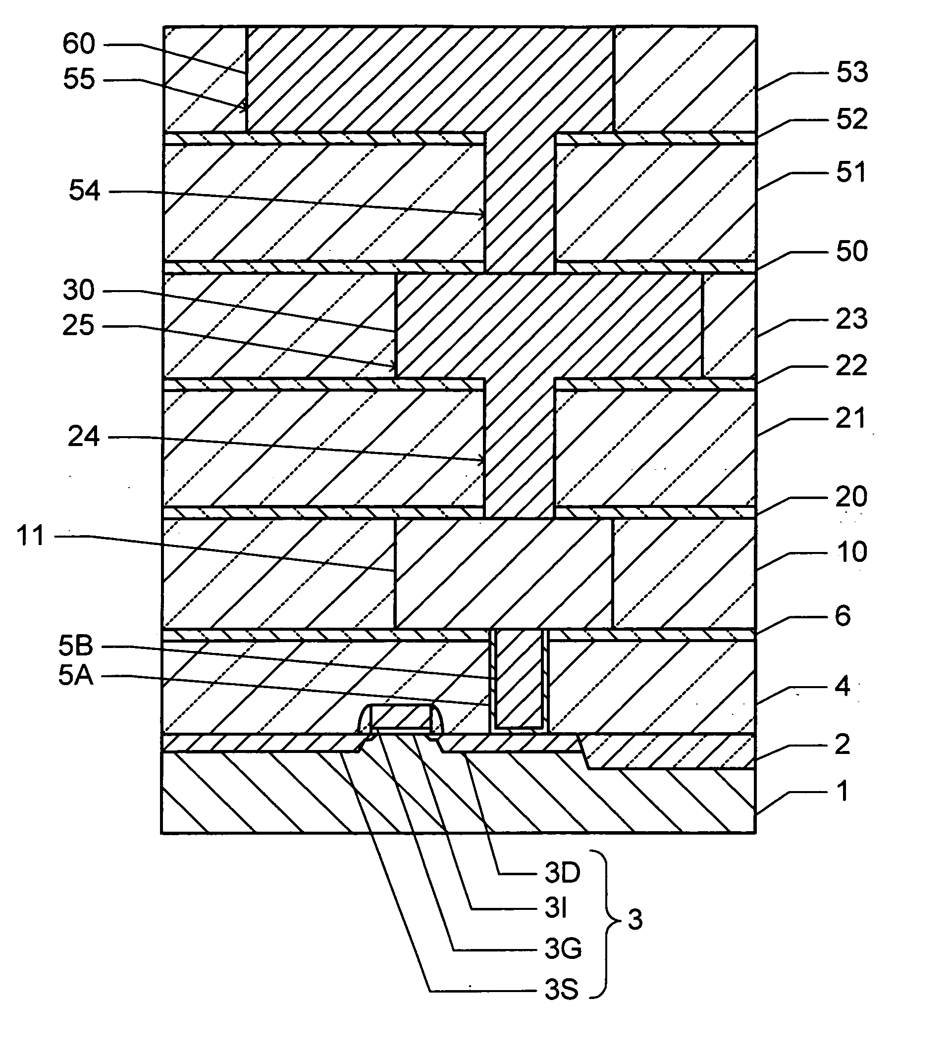
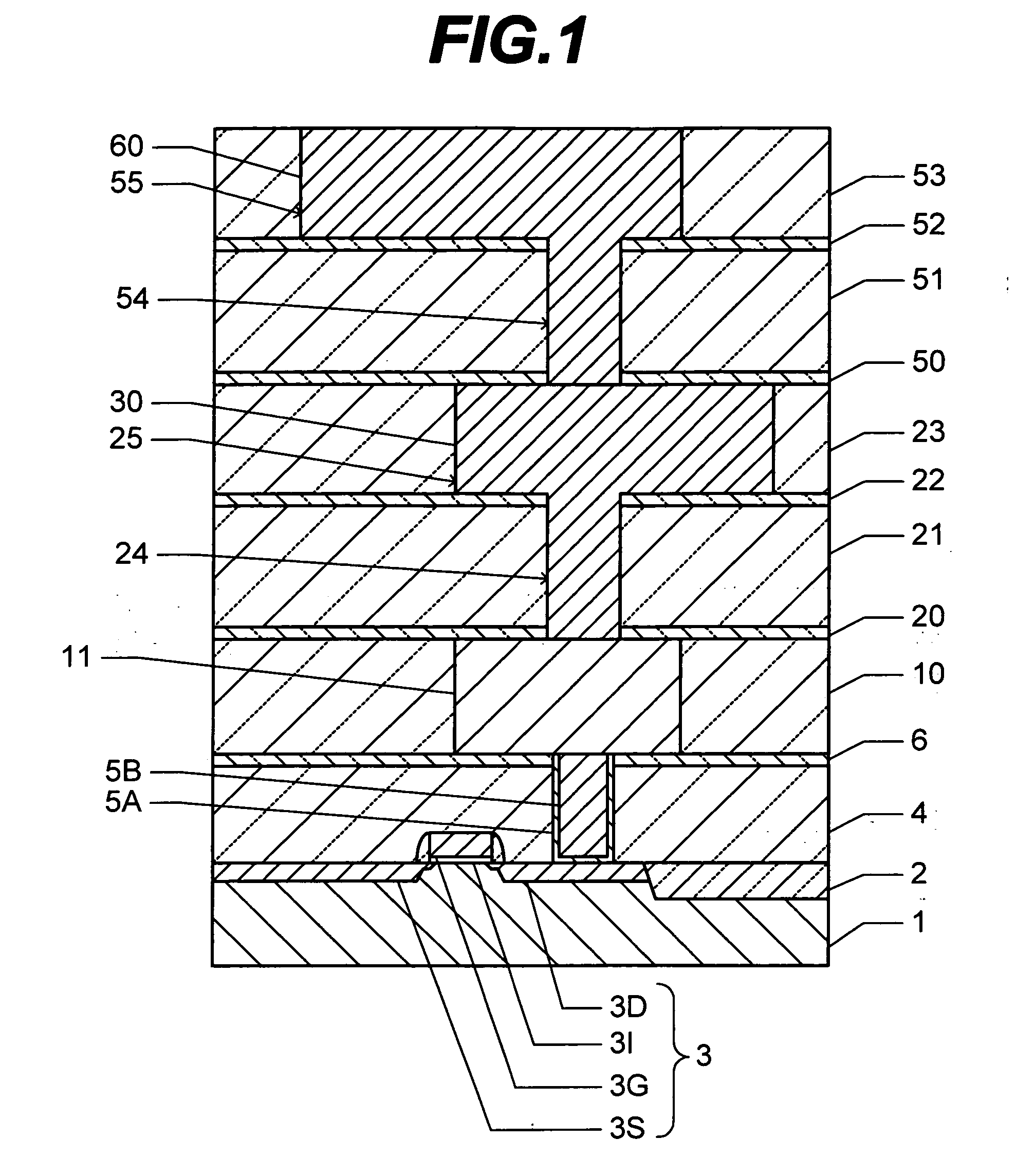
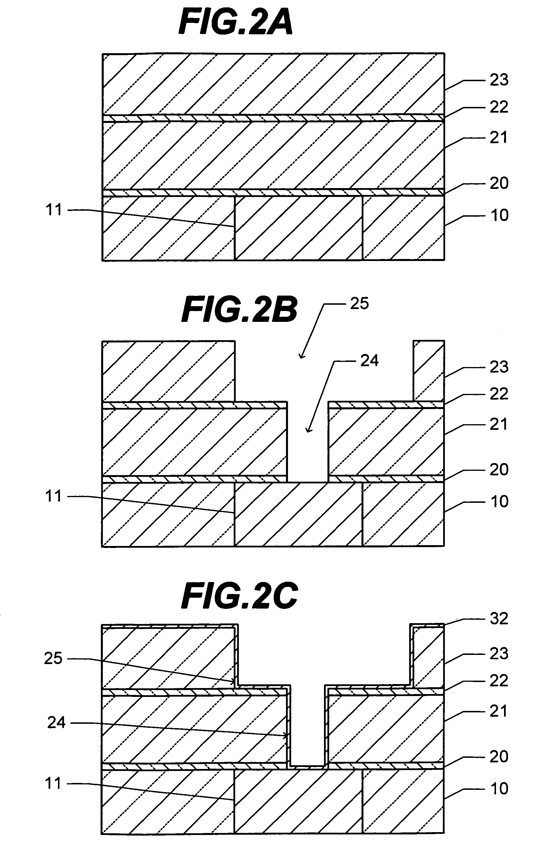
[0046] In the first embodiment, the barrier layer 34 and cover film 35 are formed by annealing in the atmosphere of inert gas added with B2H6. Instead of B2H6, annealing may be performed in an atmosphere added with PH3. If PH3 is added, a cover film 35 is made of manganese phosphide (Mn3P2, MnP, etc.).
[0047]FIG. 3 is a graph showing the relation between a concentration of additive in an annealing atmosphere and a resistivity of the conductive member 33 after annealing. The abscissa represents an additive concentration in an annealing atmosphere in the unit of “volume %” and the ordinate represents a resistivity of the conductive member 33 in the unit of “μΩcm”. Triangle and square symbols in FIG. 3 indicate resistivity of the conductive member when using B2H6 and PH3 as additive. For comparison, resistivity of the conductive member with oxygen being added to the annealing atmosphere is indicated by rhombus symbols. The annealing temperature was 300° C. and the annealing time was 30...
PUM
 Abstract
Description
Claims
Application Information
 - R&D Engineer
- R&D Manager
- IP Professional
- Industry Leading Data Capabilities
- Powerful AI technology
- Patent DNA Extraction
Browse by: Latest US Patents, China's latest patents, Technical Efficacy Thesaurus, Application Domain, Technology Topic.
© 2024 PatSnap. All rights reserved.Legal|Privacy policy|Modern Slavery Act Transparency Statement|Sitemap