

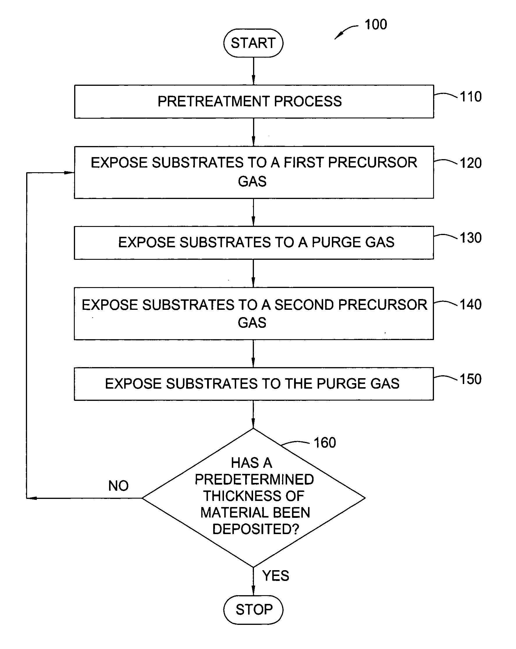
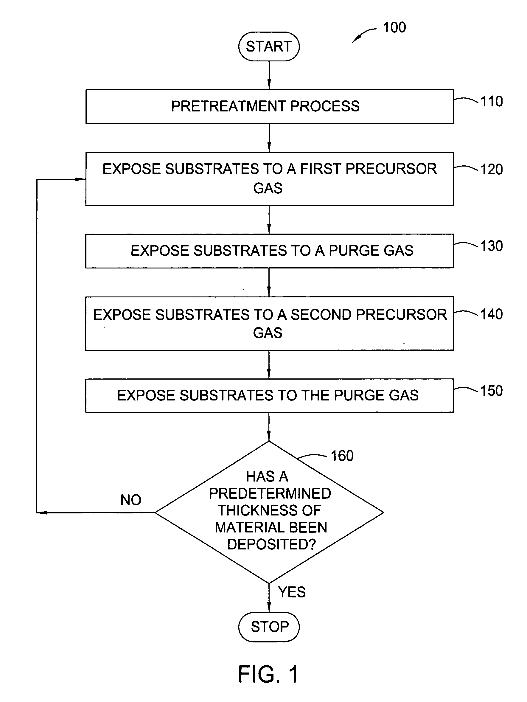
Pretreatment processes within a batch ALD reactor
a batch ald reactor and pretreatment technology, applied in the field of fabrication processes, can solve the problems of reducing the overall fabrication throughput of ald process, affecting the quality of ald process,
- Summary
- Abstract
- Description
- Claims
- Application Information
AI Technical Summary
Benefits of technology
Problems solved by technology
Method used
Image

Examples
example 1
[0041] HfO2 (H2O-Soak / O3-ALD)—A batch of 50 substrates is positioned on the susceptors of a boat within the mini-batch ALD chamber. The process chamber is maintained at a pressure of about 8 Torr at about 250° C. and exposed to a pretreatment gas containing water vapor for about 20 minutes. Thereafter, a hafnium oxide layer is formed during an ALD process by sequentially exposing the substrates to a hafnium precursor (TDMAH in nitrogen carrier gas) and ozone (15 at % ozone in oxygen). The substrates are heated to about 250° C. and exposed to a plurality of ALD cycles. Each ALD cycle includes flowing TDMAH into the chamber for about 30 seconds, evacuating the chamber for about 30 seconds, flowing nitrogen (purge gas) into the chamber for about 30 seconds, evacuating the chamber for about 30 seconds, flowing ozone into the chamber for about 30 seconds, evacuating the chamber for about 30 seconds, flowing nitrogen into the chamber for about 30 seconds and evacuating the chamber for abo...
example 2
[0042] HfO2 (O3-Soak / H2O-ALD)—A batch of 50 substrates is positioned on the susceptors of a boat within the mini-batch ALD chamber. The process chamber is maintained at a pressure of about 6 Torr at about 200° C. and exposed to a pretreatment gas containing ozone (15 at % ozone in oxygen) for about 5 minutes. Thereafter, a hafnium oxide layer is formed during an ALD process by sequentially exposing the substrates to a hafnium precursor (TDMAH in nitrogen carrier gas) and water vapor (in nitrogen carrier gas). The substrates are heated to about 200° C. and exposed to a plurality of ALD cycles. Each ALD cycle includes flowing TDMAH into the chamber for about 30 seconds, evacuating the chamber for about 30 seconds, flowing nitrogen (purge gas) into the chamber for about 30 seconds, evacuating the chamber for about 30 seconds, flowing water vapor into the chamber for about 30 seconds, evacuating the chamber for about 30 seconds, flowing nitrogen into the chamber for about 30 seconds and...
example 3
[0043] HfSiO4 (O3-Soak / H2O-ALD)—A batch of 50 substrates is positioned on the susceptors of a boat within the mini-batch ALD chamber. The process chamber is maintained at a pressure of about 8 Torr at about 300° C. and exposed to a pretreatment gas containing ozone (15 at % ozone in oxygen) for about 10 minutes. Thereafter, a hafnium silicate layer is formed during an ALD process by sequentially exposing the substrates to a hafnium precursor (TDMAH in nitrogen carrier gas), water vapor, a silicon precursor (Tris-DMAS in nitrogen carrier gas) and water vapor. The substrates are heated to about 300° C. and exposed to a plurality of ALD cycles. Each ALD cycle includes flowing TDMAH into the chamber for about 30 seconds, evacuating the chamber for about 30 seconds, flowing nitrogen (purge gas) into the chamber for about 30 seconds, evacuating the chamber for about 30 seconds, flowing water vapor into the chamber for about 30 seconds, evacuating the chamber for about 30 seconds, flowing ...
PUM
| Property | Measurement | Unit |
|---|---|---|
| Time | aaaaa | aaaaa |
| Time | aaaaa | aaaaa |
| Time | aaaaa | aaaaa |
Abstract
Description
Claims
Application Information