Semiconductor integrated circuit device and high frequency power ampifier module

a technology of integrated circuit and amplifier module, which is applied in the direction of pulse technique, process and machine control, instruments, etc., can solve problems such as new problems, achieve the effects of preventing the delay in the rise of output power, improving the characteristic of harmonic distortion of the antenna connection switching circuit, and improving the reliability of an electronic system such as communication equipmen

Active Publication Date: 2007-03-01
MURATA MFG CO LTD
View PDF1 Cites 15 Cited by
  • Summary
  • Abstract
  • Description
  • Claims
  • Application Information

AI Technical Summary

Benefits of technology

[0046] (1) A delay in the rising of an output power can be prevented, while the characteristic of harmonic distortion of an antenna connection switching circuit is improved.
[0047] (2) By constructing a high frequency power amplifier module by using the antenna connection switching circuit mentioned above in the effect (1), the reliability of an electronic system such as communication equipment can be improved.

Problems solved by technology

However, it was found by the present inventors that the above-mentioned improvement technology for reducing the harmonic distortion in the SPDT switch had the following problems.
To develop diversified services, a communication mode termed DTM (Dual Transfer Mode), which uses the voice communication and the EDGE mode in one and the same frame, has been introduced in recent years and has caused a new problem.

Method used


Image

  • Semiconductor integrated circuit device and high frequency power ampifier module
  • Semiconductor integrated circuit device and high frequency power ampifier module
  • Semiconductor integrated circuit device and high frequency power ampifier module

Examples


Embodiment Construction

[0064] Referring now to the drawings, the embodiments of the present invention will be described herein below in detail. Throughout the drawings for illustrating the embodiments, like parts are designated by like reference numerals in principle and the repeated description thereof will be omitted.

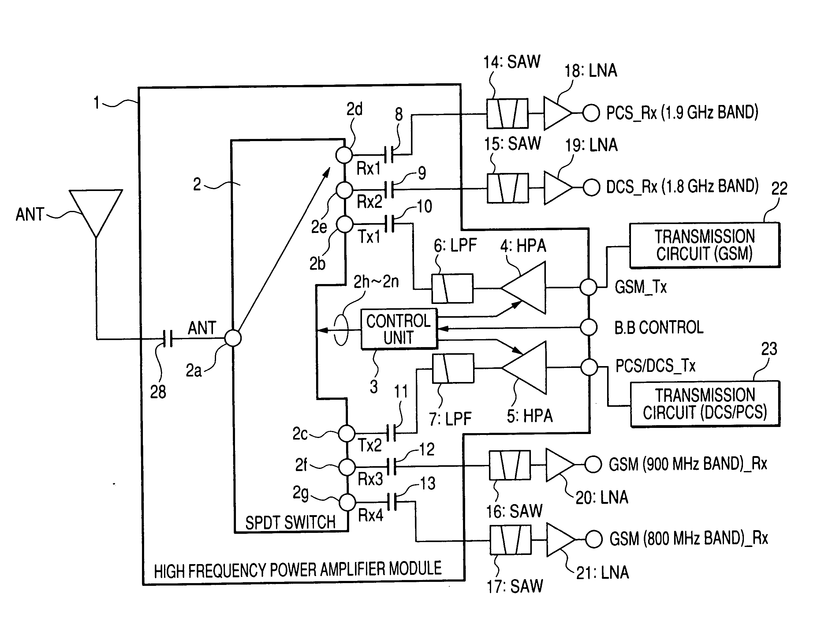
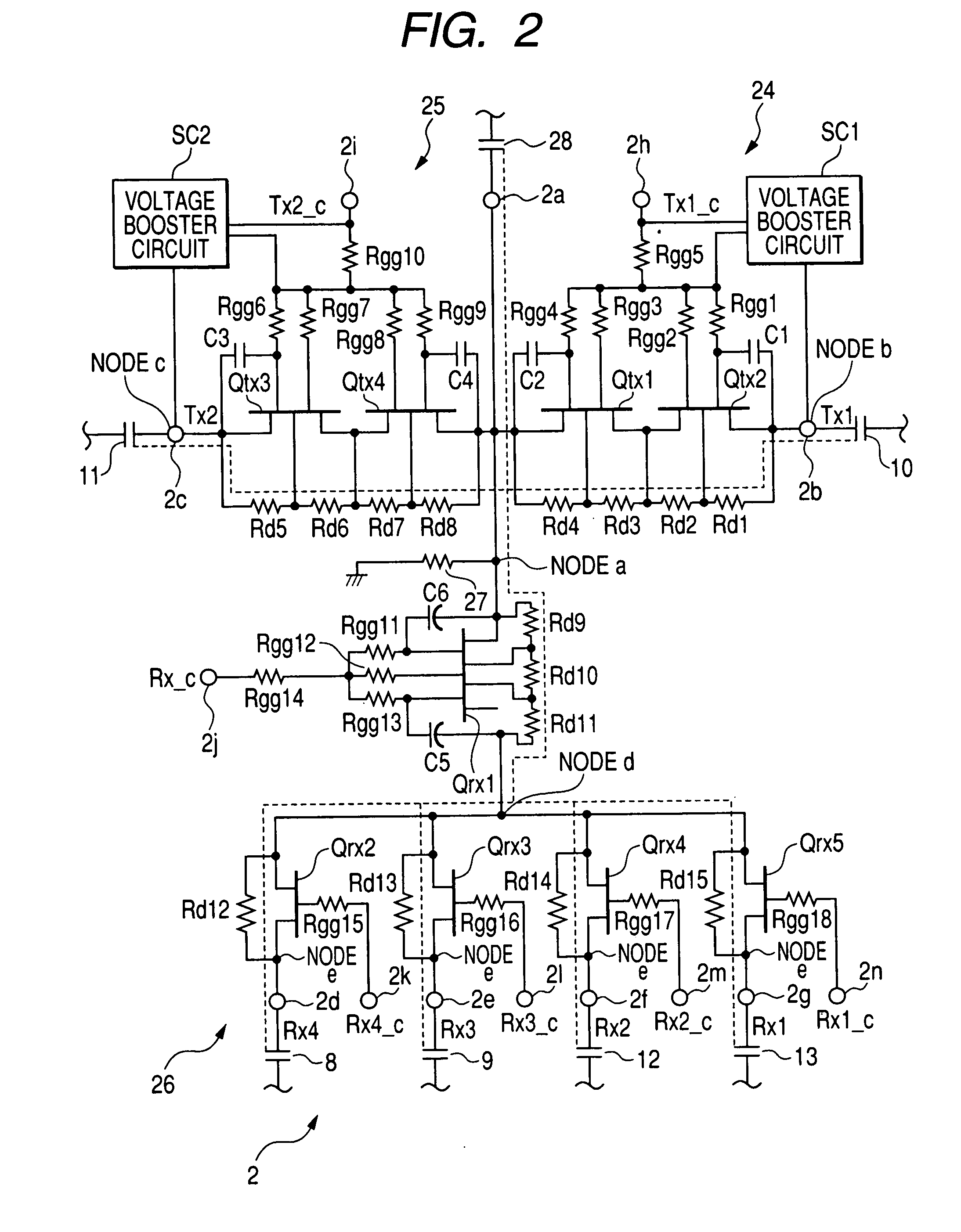
[0065]FIG. 1 is a block diagram of a high frequency power amplifier module according to an embodiment of the present invention. FIG. 2 is a circuit diagram of a SPDT switch provided in the high frequency power amplifier module of FIG. 1. FIG. 3 is a circuit diagram showing an example of a structure of a SPDT switch examined by the present inventors. FIGS. 4A and 4B are illustrative views each showing an example of the result of simulation exhibiting a response characteristic in the SPDT switch of FIG. 3. FIGS. 5A and 5B are illustrative views each showing the result of simulating time-lapse variations in gate potential Vg and drain potential Vant in the SPDT switch of FIG. 2. FIG. 6 is an ...


PUM


Abstract

In a SPDT switch, a resistor for leak path is connected between a terminal for antenna and a reference potential. The resistor for leak path allows charge capacitances accumulated in electrostatic capacitor elements provided as DC cut capacitors connected to transmission signal terminals and reception signal terminals to be discharged and allows rapid lowering of a potential at the terminal for antenna. In the SPDT switch, a switching characteristic is improved and a delay in the rising edge of a low-power slot which comes after a high-power slot is reduced.

Description

CROSS-REFERENCE TO RELATED APPLICATION [0001] The present application claims priority from Japanese patent application No. 2005-250497 filed on Aug. 31, 2005, the content of which is hereby incorporated by reference into this application. BACKGROUND OF THE INVENTION [0002] The present invention relates to a semiconductor integrated circuit device mounted on mobile communication equipment or the like and, more particularly, to a technology which is effective in reducing the distortion of a transmission / reception signal. [0003] In recent years, mobile phones have developed a wide variety of services using data communication in addition to voice communication and are still continuing to evolve. [0004] The representative frequency bands used by mobile phone services in Europe are the 900 MHz band for the GSM (Global System for Mobile Communicator) and the 1.8 GHz band for the DCS (Digital Cellular System), while the 1.9 GHz band for the PCS (Personal Communication Service) and the 850 M...

Claims


Application Information

Patent Timeline
Patent Type & Authority Applications(United States)
IPC IPC(8): H04B1/28H04B1/38
CPCH04B1/006
Inventor NAKAJIMA, AKISHIGESHIGENO, YASUSHIOGAWA, TAKASHIOSAKABE, SHINYAISHIKAWA, TOMOYUKI
Owner MURATA MFG CO LTD
Why Eureka
Try Eureka