Near-field electromagnetic wave absorber

a near-field electromagnetic and absorber technology, applied in the direction of loop antennas, electrical apparatus, antennas, etc., can solve the problems of inability to show sufficient absorption characteristics against a frequency range of several hundred mhz to 1 ghz or more where emi countermeasures, and the method of preparing an electromagnetic wave absorber by dispersing magnetic particles uniformly in the substrate is not easy, so as to achieve easy manufacturing and reduce manufacturing costs.

Inactive Publication Date: 2007-03-08
NISCA KK
View PDF15 Cites 4 Cited by
  • Summary
  • Abstract
  • Description
  • Claims
  • Application Information

AI Technical Summary

Benefits of technology

[0016] Further, in addition to the above-described object, another object of the present invention is to provide an inexpensive near-field electromagnetic wave absorber.
[0017] More, in addition to t

Problems solved by technology

Although the technique in Patent Document 1, wherein a magnetic substance is used, shows a sufficient absorption characteristic against unnecessary electromagnetic waves of a frequency range of 3 GHz or thereabout, it does not show a sufficient absorption characteristic against a frequency range of several hundred MHz to 1 GHz or more where EMI countermeasures are currently most needed.
Also, the method for preparing an electromagnetic wave absorber by dispersing the magnetic particles uniformly in the substrate is not easy,

Method used


Image

  • Near-field electromagnetic wave absorber
  • Near-field electromagnetic wave absorber
  • Near-field electromagnetic wave absorber

Examples


example 1

[0057] As a substrate, materials described in Table 1 were used. A dispersion solution, with the mass ratio of a carbon black (CB) to a carbon nano-fiber (CNF) described in Table 2, was prepared. The dispersion solution described in Table 2 was applied onto the substrate described in Table 1, while controlling the amount to be applied, and then the applied substrate was dried, to prepare an electromagnetic wave absorber. The surface density of conductive material, i.e. the carbon component, at the surface of the resulting electromagnetic wave absorber was measured.

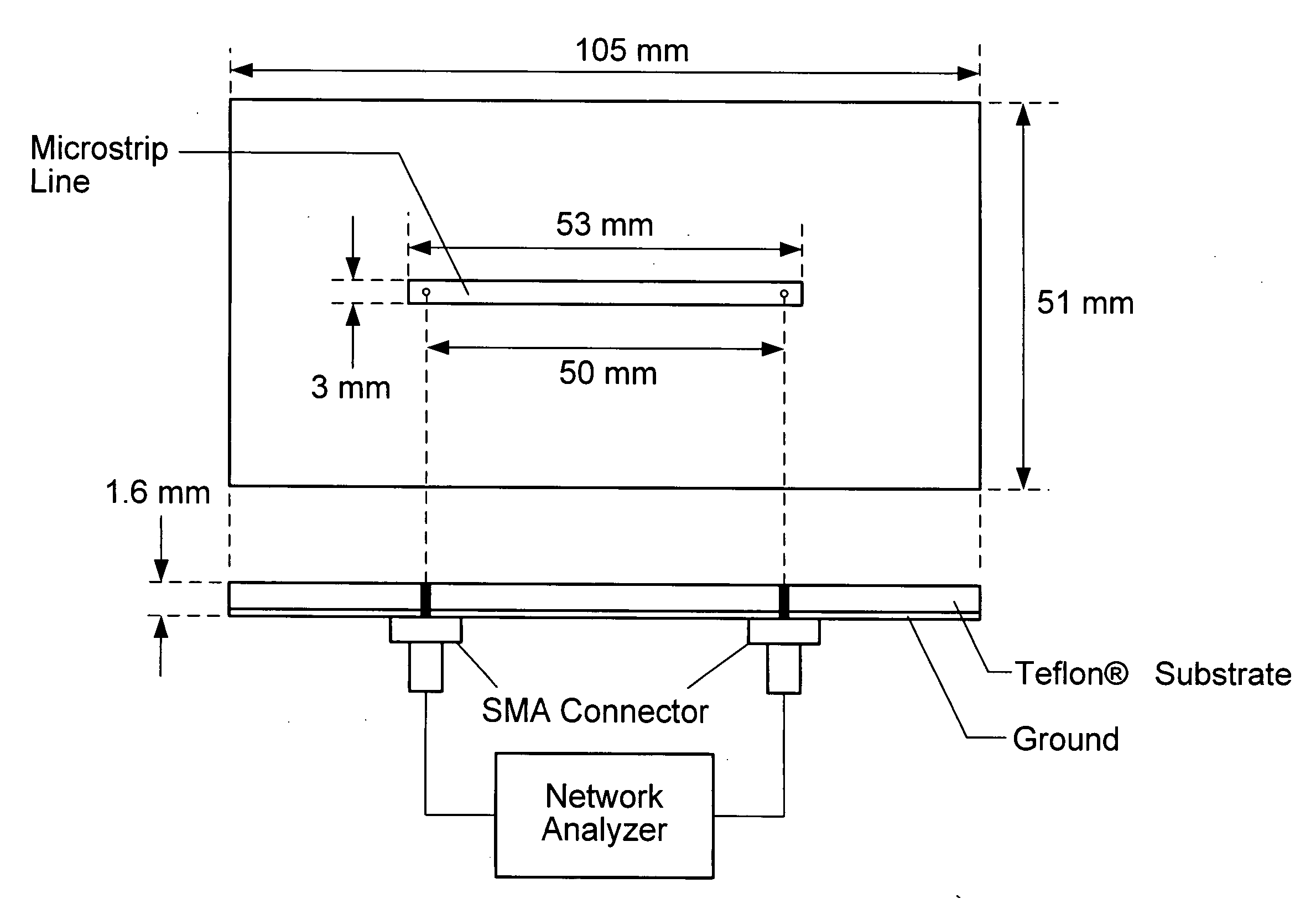
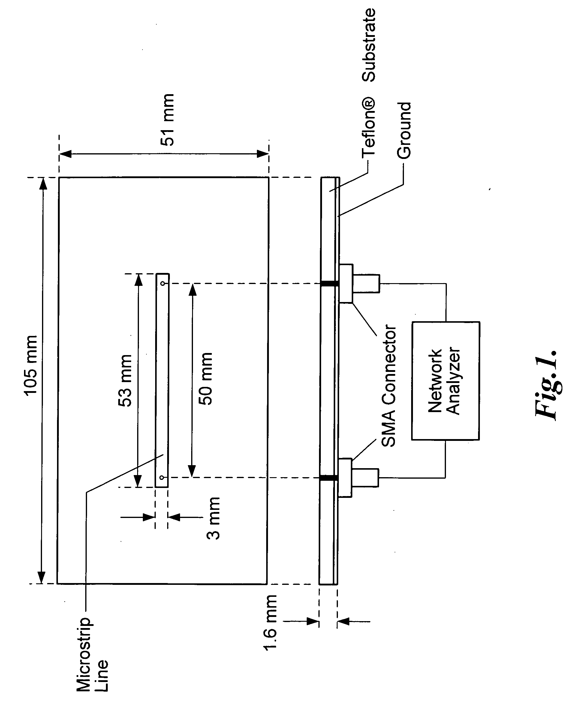
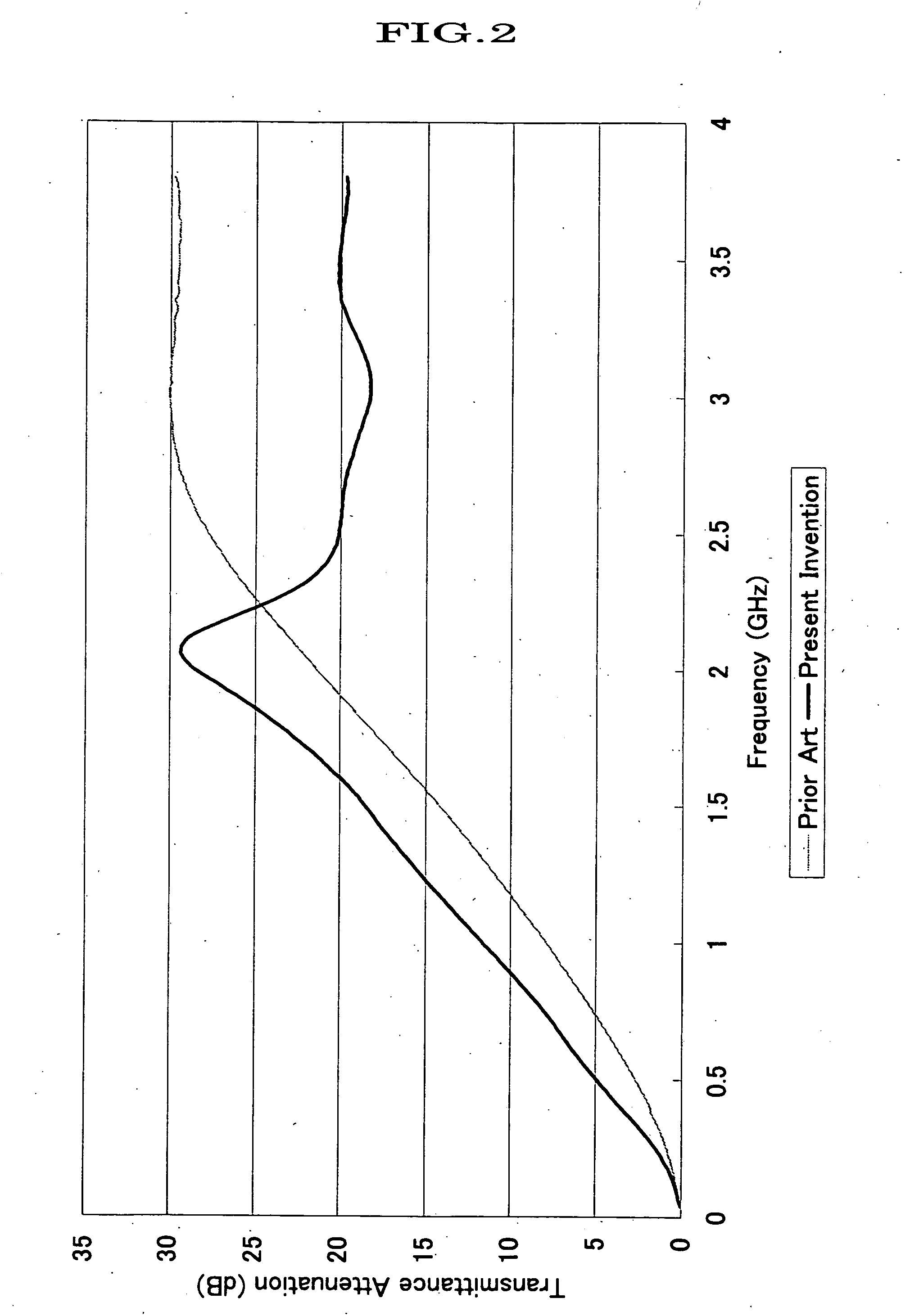
[0058] The transmission attenuation of the resulting electromagnetic wave absorber was measured in accordance with IEC TC51 WG10 standards. The measurement device was configured with a network analyzer (abbreviated hereinafter as “NA”) and a 50 Ω microstrip line (abbreviated hereinafter as “MSL”) as shown in FIG. 1.

[0059] The electromagnetic wave absorber prepared in size same as the MSL substrate (50 mm×100 mm), was adh...

example 2

[0067]

[0068] An electromagnetic wave absorber was prepared in a manner similar to in Example 1 except that “B” (No. 2 filter paper for production, manufactured by ADVANTEC TOYO KAISHA LTD.) described in Table 1 was used as a substrate, and that “4” (a mass ratio of CB / CNF=1) described in Table 2 was used as dispersion solution.

[0069] The transmission attenuation of the resulting electric wave absorber was measured in the same manner as in Example 1. The thickness of the double-faced tape used in the measurement was 20, 30, 50, 80 μm, respectively, as shown in Table 6.

[0070] Table 6 shows the surface resistivity and the transmission attenuation of the resulting electric wave absorber with the thickness of the double-faced tape used in the measurement.

[0071] Table 7 shows the transmission attenuation against an electromagnetic wave of 1 GHz depending on the thickness of the double-faced tape used in the measurement.

[0072] Further, Table 8 shows the maximum value of reflection S11 ...


PUM


Abstract

An object of the present invention is to provide a near field electromagnetic absorber that is capable of expressing an effective electromagnetic wave absorption characteristic in a broad range of frequency bands by using conductive material that conductively acts on the electrical field component of an electromagnetic wave. The present invention discloses a near-filed electromagnetic wave absorber consisting essentially of conductive material, wherein the near-field electromagnetic wave absorber absorbs an electromagnetic wave within one wavelength from the electromagnetic wave source by the conductive material, which conductively acts on the electrical field component of the electromagnetic wave.

Description

BACKGROUND OF THE INVENTION [0001] 1. Field of the Invention [0002] The present invention relates to a near-field electromagnetic wave absorber. The present invention relates to a near-field electromagnetic wave absorber having a sufficient absorption characteristic especially against an electromagnetic wave having a frequency range of several hundred MHz to 1 GHz or more. [0003] 2. Description of Related Art [0004] Conventionally, various kinds of electromagnetic wave absorbers, which suppress interference of the electromagnetic wave by absorbing an unnecessary electromagnetic wave from the noise source, have been proposed and put into practical use, in order to prevent malfunction of an electronic apparatus due to the unnecessary electromagnetic wave that is an unintended noise released from a communication apparatus and various kinds of electronic apparatuses. [0005] Electromagnetic wave absorbing materials of the electromagnetic wave absorbers may include materials using a magne...

Claims


Application Information

Patent Timeline
IPC IPC(8): H01Q17/00
CPCH01Q17/00H01Q7/00
Inventor NAKAGOMI, TAKAMITSUKOUNO, MASAHIRO
Owner NISCA KK
Why Eureka
Try Eureka