Three-phase low noise charge pump and method

a charge pump and low noise technology, applied in the field of three-phase low noise charge pump and method, can solve the problems of fast negative-going spike in vout, noise-producing transient process, and problem of internal supply generation through charge pump circuit,

Active Publication Date: 2007-03-08
TEXAS INSTR INC
View PDF1 Cites 54 Cited by
  • Summary
  • Abstract
  • Description
  • Claims
  • Application Information

AI Technical Summary

Benefits of technology

[0014] It is an object of the invention to provide an improved charge pump circuit having substantially reduced output noise.
[0015] It is another object of the invention to provide an improved charge pump without having to provide a large reservoir capacitor connected to the charge pump output conductor.
[0018] In the described embodiments, the three-phase charge pump circuit includes a second flying capacitor (C2), a third switching circuit (20A) for selectively coupling a first terminal (17) of the second flying capacitor (C2) to the first supply voltage (VCC) during a second recharging phase and to the output voltage (Vout) during a second discharging phase, a fourth switching circuit (15A) for selectively coupling a second terminal (16) of the second flying capacitor (C2) to the second supply voltage (GND) during the second recharging phase and to the first conductor (5) during the second discharging phase. A fourth switching circuit (20A) couples the second terminal (16) of the second flying capacitor (C2) to the second conductor (30) during a second parasitic capacitance precharging phase that occurs between the second recharging phase and the second discharging phase so as to cause the voltage of the first terminal (17) of the second flying capacitor (C2) to have a value that avoids noise spikes on the output conductor (10) due to charge redistribution when the first terminal (17) of the second flying capacitor (C2) is coupled to the output conductor (10). The three-phase charge pump also includes a third flying capacitor (C3), a fifth switching circuit (36) for selectively coupling a first terminal (34) of the third flying capacitor (C3) to the first supply voltage (VCC) during the third recharging phase and to the output voltage (Vout) during a third discharging phase, a sixth switching circuit (31) for selectively coupling a second terminal (33) of the third flying capacitor (C3) to the second supply voltage (GND) during the third recharging phase and to the first conductor (5) during the third discharging phase. The sixth switching circuit (31) couples the second terminal (33) of the third flying capacitor (C3) to the second conductor (30) during a third parasitic capacitance precharging phase that occurs between the third recharging phase and the third discharging phase so as to cause the voltage of the first terminal (34) of the third flying capacitor (C3) to have a value that avoids noise spikes on the output conductor (10) due to charge redistribution when the first terminal (34) of the third flying capacitor (C3) is coupled to the output conductor (10).
[0020] In the described embodiments, a first terminal (17) of a second flying capacitor (C2) is coupled to the output conductor (10) during a second discharging phase and a second terminal (16) of the second flying capacitor (C2) coupled to the discharge control circuit (2,4) to increase the voltage of the second terminal (17) of the second flying capacitor (C2) during the second discharging phase until the output voltage (Vout) is equal to the regulated value. A second terminal (33) of a third flying capacitor (C3) is coupled to a precharge control circuit (25,27) during a third parasitic capacitance precharging phase to cause the voltage of the first terminal (34) of the third flying capacitor (C3) to have a value that avoids noise spikes on the output conductor (10) due to charge redistribution when the first terminal (34) of the third flying capacitor (C3) is coupled to the output conductor (10). The first terminal (17) of the second flying capacitor (C2) is coupled to the first voltage (VCC) during a second recharging phase and the second terminal (16) of the second flying capacitor (C2) is selectively coupled to the second voltage (GND) during the second recharging phase. The first terminal (34) of the third flying capacitor (C3) is coupled to the output conductor (10) during the third discharging phase and the second terminal (33) of the third flying capacitor (C3) is coupled to the discharge control circuit (2,4) to increase the voltage of the second terminal (34) of the third flying capacitor (C3) during the third discharging phase until the output voltage (Vout) is equal to the regulated value. The second terminal (16) of the second flying capacitor (C2) is coupled to the precharge control circuit (25,27) during a second parasitic capacitance precharging phase to cause the voltage of the first terminal (17) of the second flying capacitor (C2) to have a value that avoids noise spikes on the output conductor (10) due to charge redistribution when the first terminal (17) of the second flying capacitor (C2) is coupled to the output conductor (10). The first terminal (34) of a third flying capacitor (C3) is selectively coupled to the first voltage (VCC) during a third recharging phase and the second terminal (33) of the third flying capacitor (C3) is coupled to the second voltage (GND) during the third recharging phase.

Problems solved by technology

However, generation of such an internal supply by means of a charge pump circuit has been problematic due to the large amount of output noise (at the charge-pump clock frequency) produced by known charge pumps.
A drawback of prior art two-phase charge pump circuit 1 is that it has a fast, noise-producing transient process between its above mentioned first and second phases, during which the top plate of one of the flying capacitors is connected to reservoir capacitor Cout at the same time the voltage across the associated parasitic capacitor connected between the bottom plate of that flying capacitor and ground (i.e., the integrated circuit substrate) is still at 0 volts.
This causes a fast negative-going spike in Vout, which constitutes the noise above mentioned noise.
This can typically result in negative noise spikes of roughly 70 millivolts.

Method used


Image

  • Three-phase low noise charge pump and method
  • Three-phase low noise charge pump and method
  • Three-phase low noise charge pump and method

Examples


Embodiment Construction

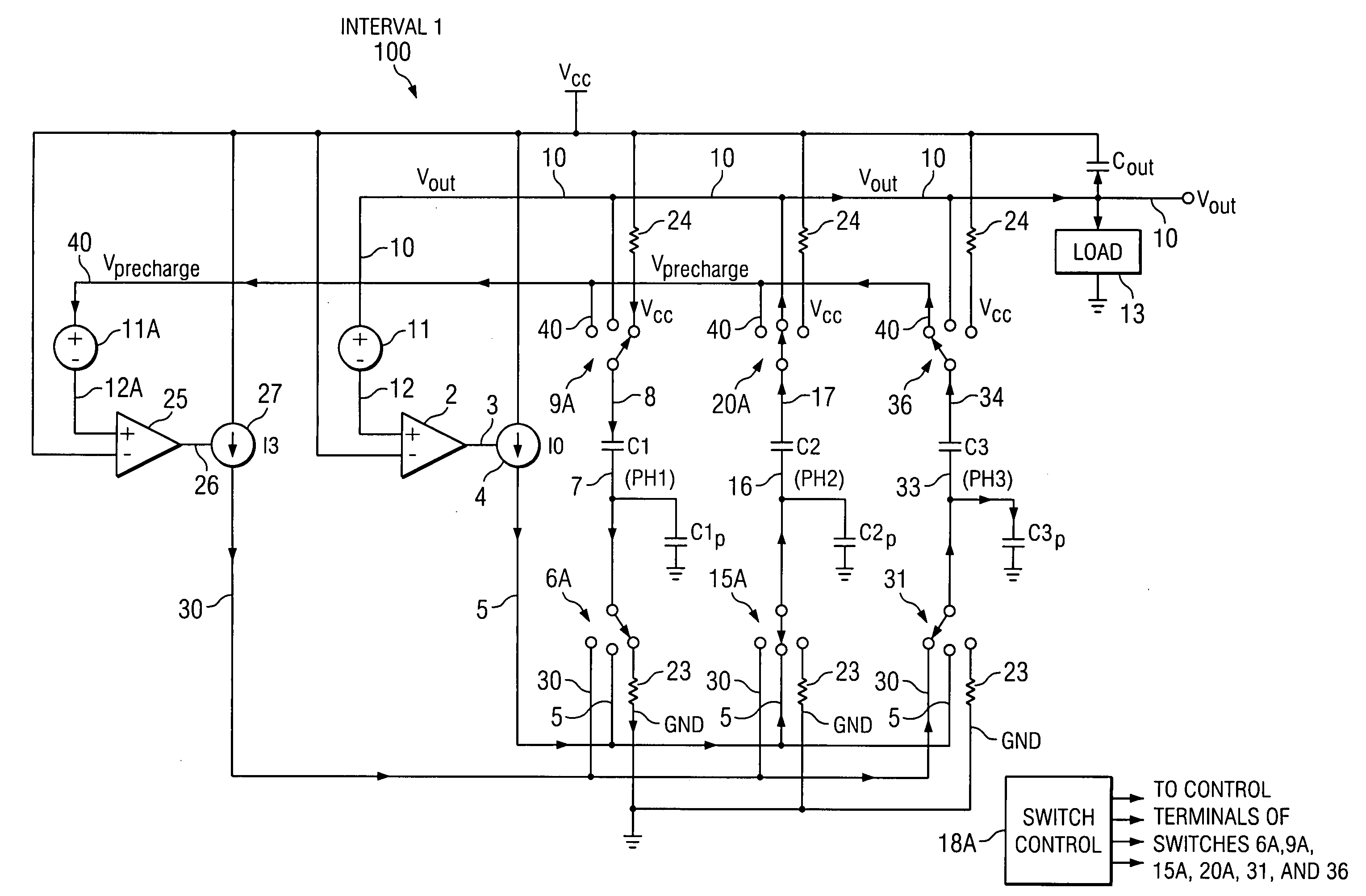
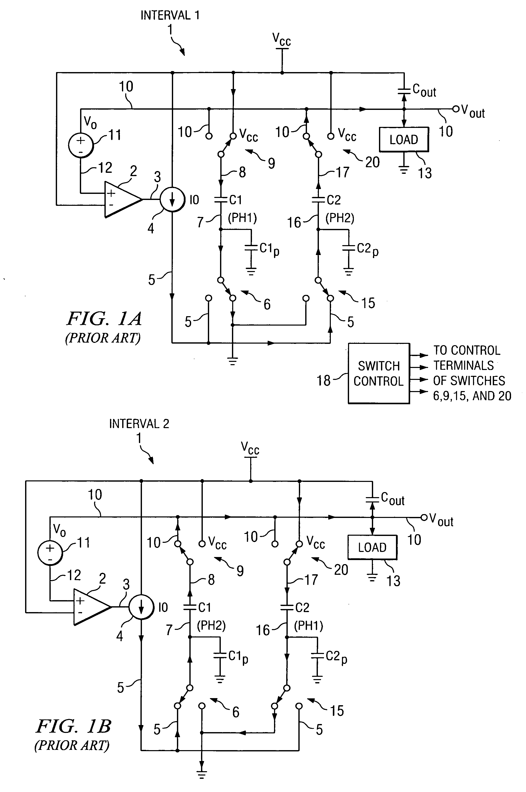
[0030] The method and structure of the present invention are utilized to provide a very low noise charge pump circuit. This is accomplished by providing a three-phase charge pump circuit 100 shown in FIG. 3A having three flying capacitors, each having three phases of operation. An additional “phase 3” (PH3) of operation of each flying capacitor and associated circuitry occurs between the previously described “phase 1” (PH1) and “phase 2” (PH2)operations of previously described prior art charge pump 1 of FIG. 1A.

[0031]FIG. 3A shows a charge pump circuit 100, which includes an amplifying circuit 2 having an output 3 connected to a control terminal of a controlled current source 4. Controlled current source 4 produces a controlled current 10, wherein the amount of controlled current 10 is determined by load demand of reservoir capacitor Cout and load 13 and also by the feedback loop being controlled through operation of amplifier 2. The (−) input of amplifier 2 is connected to VCC. Th...


PUM


Abstract

A low noise charge pump circuit includes a first terminal of a first flying capacitor selectively coupled to a first voltage during a first recharging phase and a second terminal of the first flying capacitor selectively coupled to a second voltage during the first recharging phase. The second terminal of the first flying capacitor is coupled to a precharge control circuit during a first parasitic capacitance precharging phase that occurs after the first recharging phase to cause the voltage of the first terminal of the first flying capacitor to equal an output voltage. The first terminal of the first flying capacitor is coupled to an output conductor conducting the output voltage during a first discharging phase that occurs after the first parasitic capacitance precharging phase. The second terminal of the first flying capacitor is coupled to a discharge control circuit which increases the voltage of the second terminal of the first flying capacitor during the first discharging phase until the output voltage is equal to a regulated value.

Description

BACKGROUND OF THE INVENTION [0001] The present invention relates generally to charge pumps, and more particularly to an improvement which provides substantially reduced output noise compared to prior charge pumps. [0002] On-chip generation of an internal supply voltage at a value greater than the power supply voltage rail VCC has been one approach to providing rail-to-rail operation of an operational amplifier. However, generation of such an internal supply by means of a charge pump circuit has been problematic due to the large amount of output noise (at the charge-pump clock frequency) produced by known charge pumps. [0003] A standard charge pump circuit is a two-phase circuit including two “flying capacitors” and one “reservoir capacitor” which operate to store and maintain the output voltage of the charge pump circuit. FIG. 1A shows a standard charge pump circuit 1, which includes an amplifying circuit 2 having an output 3 connected to a control terminal of a controlled current s...

Claims


Application Information

Patent Timeline
Patent Type & Authority Applications(United States)
IPC IPC(8): H02M3/18
CPCH02M2003/077H02M3/07H02M3/077
Inventor ALENIN, SERGEY
Owner TEXAS INSTR INC
Why Eureka
Try Eureka