Image defect inspection apparatus, image defect inspection system, defect classifying apparatus, and image defect inspection method

a defect inspection and defect technology, applied in the field of image defect inspection apparatus, can solve the problems of long time before electrical testing, defect classification takes a lot of processing time, and electrical testing cannot be well utilized for improving yield, so as to reduce the detection sensitivity, reduce variance, and reduce the effect of defect detection sensitivity

Inactive Publication Date: 2007-03-08
TOKYO SEIMITSU
View PDF1 Cites 34 Cited by
  • Summary
  • Abstract
  • Description
  • Claims
  • Application Information

AI Technical Summary

Benefits of technology

[0020] In view of the above, an image defect inspection apparatus according to a first aspect of the present invention is designed to detect a gray level difference between corresponding pixels in two inspection images and, if the gray level difference exceeds a detection threshold value, then to judge that one or the other of the pixels in the two inspection images represents a defect, the apparatus comprising: a variance computing unit which computes the variance of the coordinate value of the pixel by weighting the coordinate value in accordance with the gray level difference detected for the pixel (or with binarized information generated by binarizing the gray level difference); and a detection sensitivity reducing unit which reduces detection sensitivity for the defect the variance increases.
[0021] The detection sensitivity reducing unit may reduce the defect detection sensitivity by correcting the detection threshold value in accordance with the computed variance. Further, the image defect inspection apparatus may output the variance together with defect information concerning the detected defect.

Problems solved by technology

However, as the semiconductor fabrication process consists of many process steps, it takes a very long time before the electrical testing can be conducted after the start of the fabrication process; as a result, when, for example, process steps are found faulty as a result of the electrical testing, many wafers are already partway through the process, and the result of the electrical testing cannot be well utilized for improving the yield.
The defect classification takes much processing time because each defective portion needs to be examined in detail.
However, when the noise level contained in the inspection image has a large dependency on the inspection image, the distribution of the gray level difference greatly differs depending on the inspection image and, in such cases, it has been difficult to suppress the occurrence of false defects even if the threshold value is determined for each inspection image as described above.

Method used


Image

  • Image defect inspection apparatus, image defect inspection system, defect classifying apparatus, and image defect inspection method
  • Image defect inspection apparatus, image defect inspection system, defect classifying apparatus, and image defect inspection method
  • Image defect inspection apparatus, image defect inspection system, defect classifying apparatus, and image defect inspection method

Examples


first embodiment

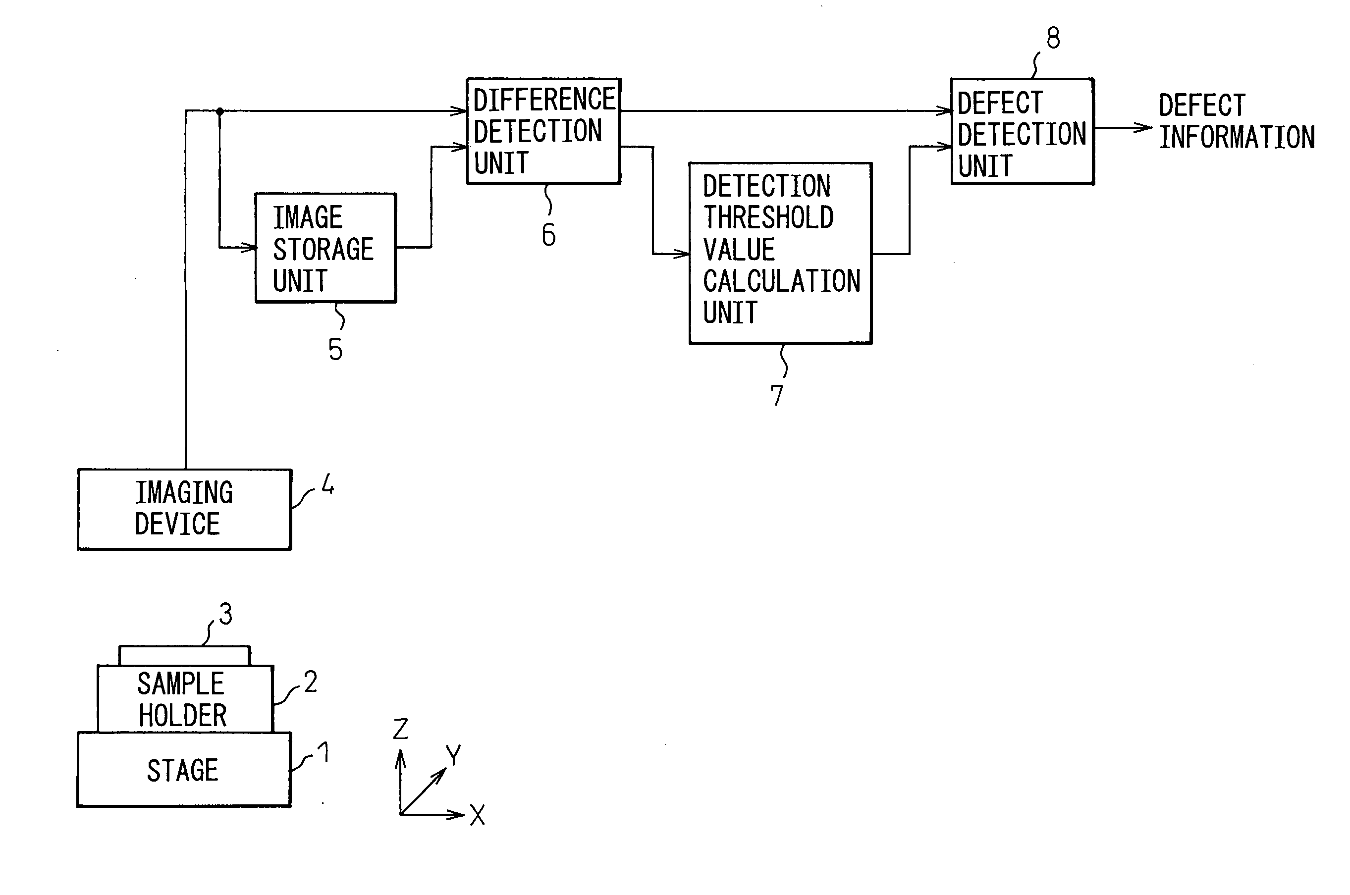
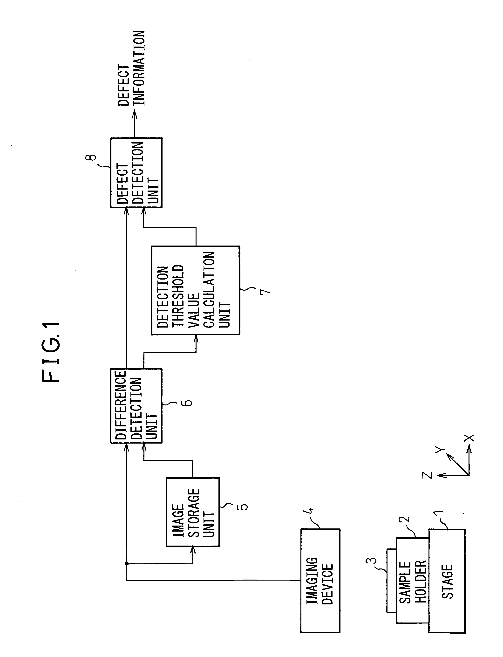
[0043]FIG. 3 is a block diagram of an appearance inspection apparatus according to an image defect inspection apparatus of the present invention. The appearance inspection apparatus shown in FIG. 3 is similar in configuration to the prior art appearance inspection apparatus described with reference to FIG. 1; therefore, the same component elements are designated by the same reference numerals, and the description thereof will not be repeated here.

[0044] The difference detection unit 6 detects differences (gray level differences) between the pixel values (gray level signals) of the corresponding pixels contained in corresponding portions of two images captured of two dies (one image is taken as an inspection image, and the other as a reference image), and creates a difference image by mapping the difference signals to pixel values.

[0045] The appearance inspection apparatus 10 includes a variance computing unit 21 which takes as an input the difference image created by the difference...

second embodiment

[0066]FIG. 6 is a block diagram of an appearance inspection apparatus according to the image defect inspection apparatus of the present invention. In the embodiment shown in FIG. 6, the variance computing unit 21 computes the variance of the coordinate value of each pixel weighted in accordance with binarized information generated by binarizing the pixel value (gray level difference signal) of each pixel in the difference image created by the difference detection unit 6. In this method of variance computation, as the computation is performed only on pixels for which the binarized gray level difference signal has one or the other of the two values, the variance can be computed in a simpler manner.

[0067] In this case, the defect detection unit 8 compares each pixel in the difference image created by the difference detection unit 6 with the threshold value calculated by the detection threshold value calculation unit 7 and, if the gray scale difference exceeds the threshold value, then ...

third embodiment

[0074]FIG. 8 is a block diagram of an appearance inspection apparatus according to the image defect inspection apparatus of the present invention in the appearance inspection system shown in FIG. 7. The appearance inspection apparatus 10 supplies the variance information computed by the variance computing unit 21 to the automatic defect classifying apparatus 50 at the next stage together with (or by including therein) the defect information created by the defect detection unit 8.

[0075]FIG. 9 is a block diagram showing an embodiment of the automatic defect classifying apparatus according to the present invention shown in FIG. 7. The automatic defect classifying apparatus 50 comprises a data input unit 51 to which the defect information and variance information output from the appearance inspection apparatus 10 are input, and a classifying unit 52 in which the defect information output from the appearance inspection apparatus 10 is classified according to various parameters contained ...


PUM


Abstract

An image defect inspection apparatus, which detects a gray level difference between corresponding pixels in two inspection images and which, if the gray level difference exceeds a detection threshold value, judges that one or the other of the pixels in the two inspection images represents a defect, comprises: a variance computing unit which computes the variance of the coordinate value of the pixel by weighting the coordinate value in accordance with the gray level difference detected for the pixel; and a detection sensitivity reducing unit which reduces the detection sensitivity for the defect as the variance increases.

Description

BACKGROUND OF THE INVENTION [0001] 1. Field of the Invention [0002] The present invention relates to an image defect inspection apparatus, an image defect inspection system, and an image defect inspection method which detect a gray level difference between corresponding portions of two images, compare the detected gray level difference with a threshold value, and judge the portion under inspection to be a defect if the gray level difference is larger than the threshold value; the invention also relates to a defect classifying apparatus for classifying the thus detected defect. [0003] 2. Description of the Related Art [0004] The present invention is directed to an image processing method and apparatus which compares corresponding portions between two images that should be the same, and judges the portion under inspection to be a defect if the difference is large. The description herein is given by taking, as an example, an appearance inspection apparatus for detecting defects in a se...

Claims


Application Information

Patent Timeline
Patent Type & Authority Applications(United States)
IPC IPC(8): G06K9/00
CPCG06T2207/30148G06T7/001
Inventor ISHIKAWA, AKIO
Owner TOKYO SEIMITSU
Why Eureka
Try Eureka