Method of forming polycrystalline silicon thin film and method of manufacturing thin film transistor using the method

a technology of polycrystalline silicon and thin film, which is applied in the direction of basic electric elements, electrical equipment, semiconductor devices, etc., to achieve the effect of improving electrical characteristics

Active Publication Date: 2007-03-08
SAMSUNG DISPLAY CO LTD
View PDF4 Cites 37 Cited by
  • Summary
  • Abstract
  • Description
  • Claims
  • Application Information

AI Technical Summary

Benefits of technology

[0012] The present invention provides a method of forming a polycry

Problems solved by technology

However, the polycrystalline silicon thin film is composed of grains with all crysta

Method used


Image

  • Method of forming polycrystalline silicon thin film and method of manufacturing thin film transistor using the method
  • Method of forming polycrystalline silicon thin film and method of manufacturing thin film transistor using the method
  • Method of forming polycrystalline silicon thin film and method of manufacturing thin film transistor using the method

Examples


Embodiment Construction

[0025] The present invention is described below more fully with reference to the accompanying drawings, in which preferred embodiments of this invention are shown. Advantages and features of the present invention and methods of accomplishing the same may be understood more readily by reference to the following detailed description of preferred embodiments and the accompanying drawings. The present invention may, however, be embodied in many different forms and should not be construed as being limited to the embodiments set forth herein. Rather, these embodiments are provided so that this disclosure will be thorough and complete and will fully convey the concept of the invention to those skilled in the art, and the present invention will only be defined by the appended claims. Like reference numerals refer to like elements throughout the specification.

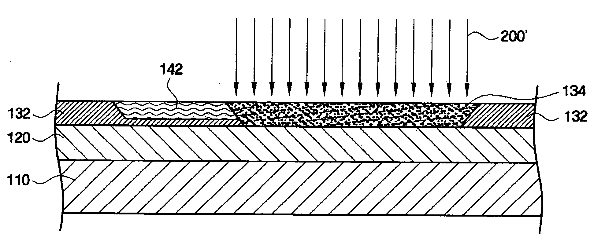
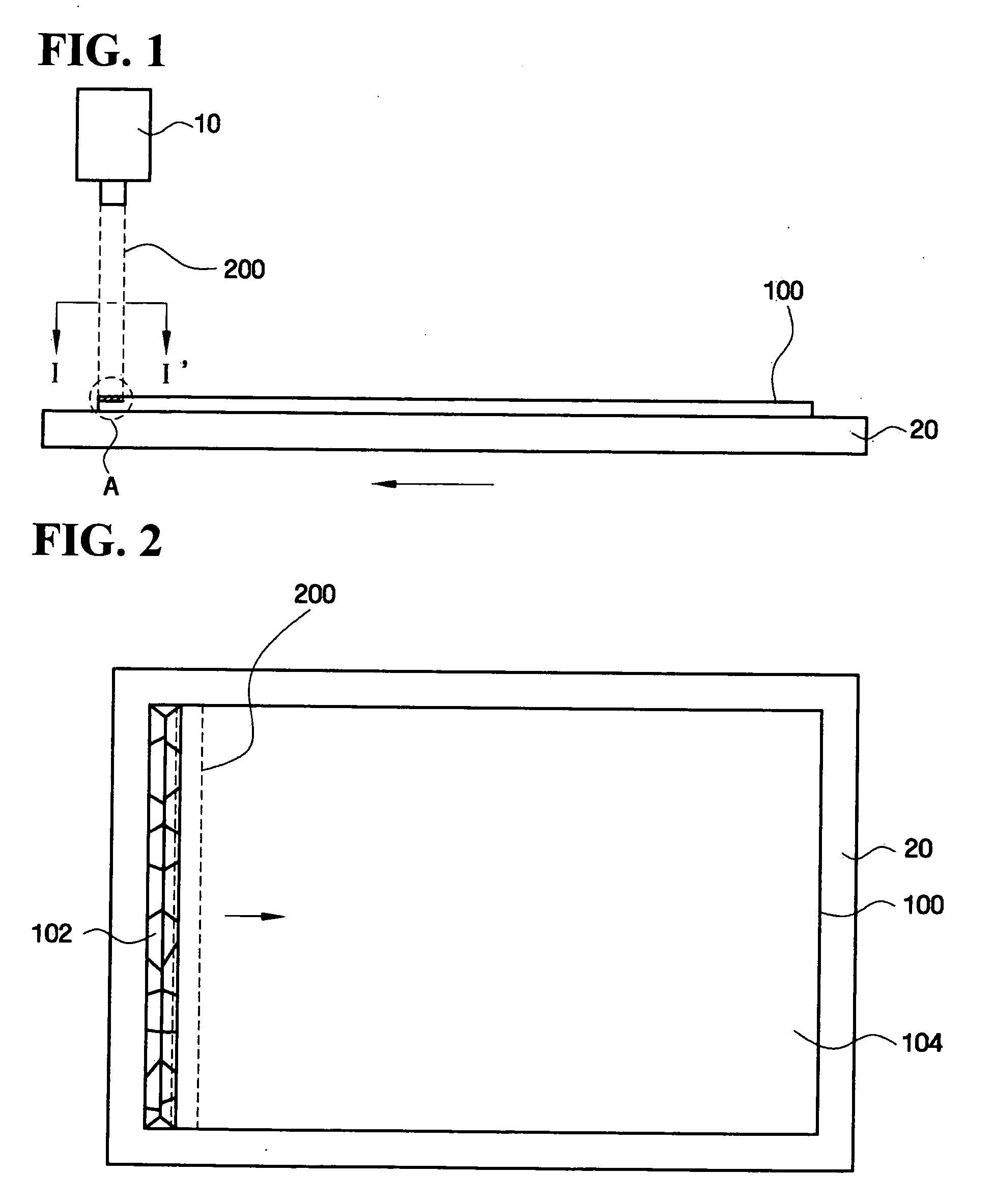
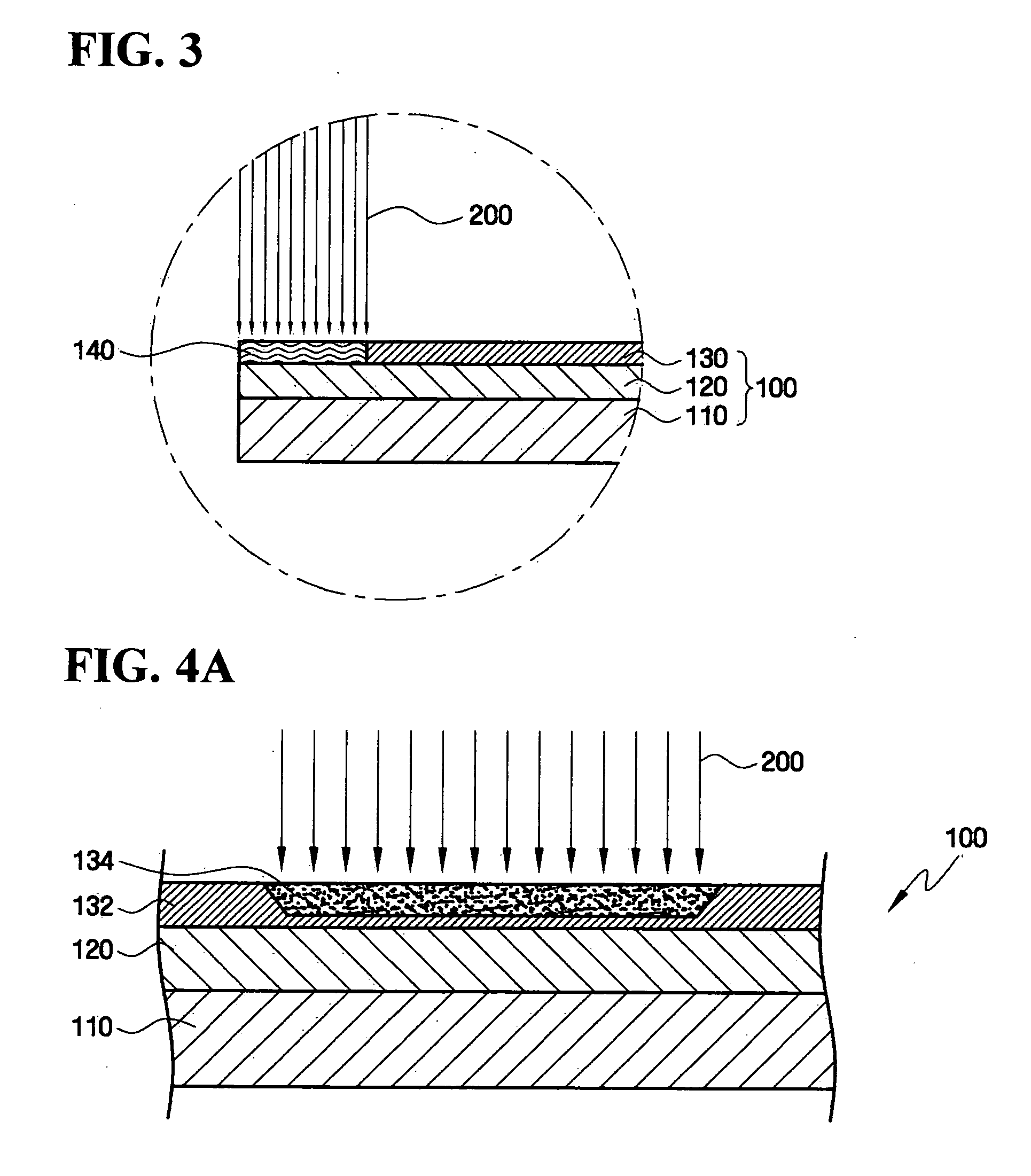
[0026]FIG. 1 is a side view illustrating an apparatus used in a method of forming a polycrystalline silicon thin film according to an...


PUM


Abstract

Provided are a method of forming a polycrystalline silicon thin film with improved electrical characteristics and a method of manufacturing a thin film transistor using the method of forming the polycrystalline silicon thin film. The method includes forming an amorphous silicon thin film on a substrate, partially melting a portion of the amorphous silicon thin film by irradiating the portion of the amorphous silicon thin film with a laser beam having a low energy density, forming polycrystalline silicon grains with a predetermined crystalline arrangement by crystallizing the partially molten portion of the amorphous silicon thin film, completely melting a portion of the polycrystalline silicon grains and a portion of the amorphous silicon thin film by irradiation of a laser beam having a high energy density while repeatedly moving the substrate by a predetermined distance, and growing the polycrystalline silicon grains by crystallizing the completely molten silicon homogeneously with the predetermined crystalline arrangement.

Description

[0001] This application claims priority from Korean Patent Application No. 10-2005-0076347 filed on Aug. 19, 2005 in the Korean Intellectual Property Office, the disclosure of which is incorporated herein by reference in its entirety. BACKGROUND OF THE INVENTION [0002] 1. Field of the Invention [0003] The present invention relates to a method of forming a polycrystalline silicon thin film with improved electrical characteristics and a method of manufacturing a thin film transistor using the method. [0004] 2. Description of the Related Art [0005] A general liquid crystal display uses an amorphous silicon thin film transistor (a-Si TFT) as a switching element. In recent years, with the demand for high-definition display quality LCDs, a polycrystalline silicon thin film transistor (poly-Si TFT) having a high driving speed is widely used. [0006] In the poly-Si TFT, various methods for forming the poly-Si thin film are well known. Of the different types of methods for forming poly-Si, th...

Claims


Application Information

Patent Timeline
IPC IPC(8): H01L21/20
CPCH01L21/2026H01L27/1285H01L29/045H01L21/02422H01L21/02686H01L21/02532H01L21/02675H01L27/1214
Inventor KIM, DONG-BYUMCHUNG, SE-JIN
Owner SAMSUNG DISPLAY CO LTD
Why Eureka
Try Eureka