Transparent thin film transistor (TFT) and its method of manufacture

a thin film transistor and transparent technology, applied in the direction of instruments, semiconductor devices, electrical apparatus, etc., can solve the problems of reducing the aperture ratio of tft, increasing power consumption, and deteriorating tft, so as to improve the resolution of the display and improve the aperture ratio

Inactive Publication Date: 2007-03-15
SAMSUNG MOBILE DISPLAY CO LTD
View PDF14 Cites 281 Cited by
  • Summary
  • Abstract
  • Description
  • Claims
  • Application Information

AI Technical Summary

Benefits of technology

[0010] Accordingly, it is an object of the present invention to provide a transparent Thin Film Transistor (TFT) in which a semiconductor layer is formed of a transparent material

Problems solved by technology

However, when the TFT is used as the switching device of the light emitting display, there are limitations on increasing the width of the channel since the amorphous silicon is op

Method used


Image

  • Transparent thin film transistor (TFT) and its method of manufacture
  • Transparent thin film transistor (TFT) and its method of manufacture
  • Transparent thin film transistor (TFT) and its method of manufacture

Examples


first embodiment

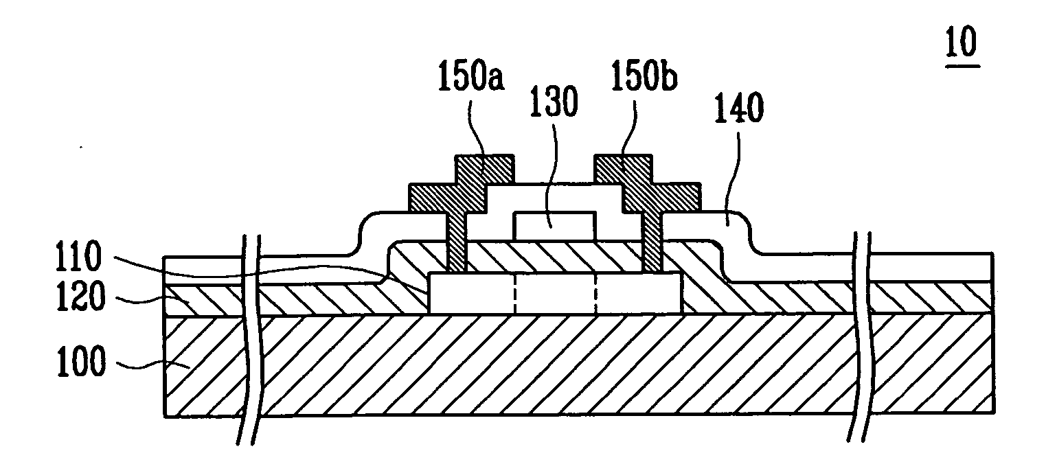
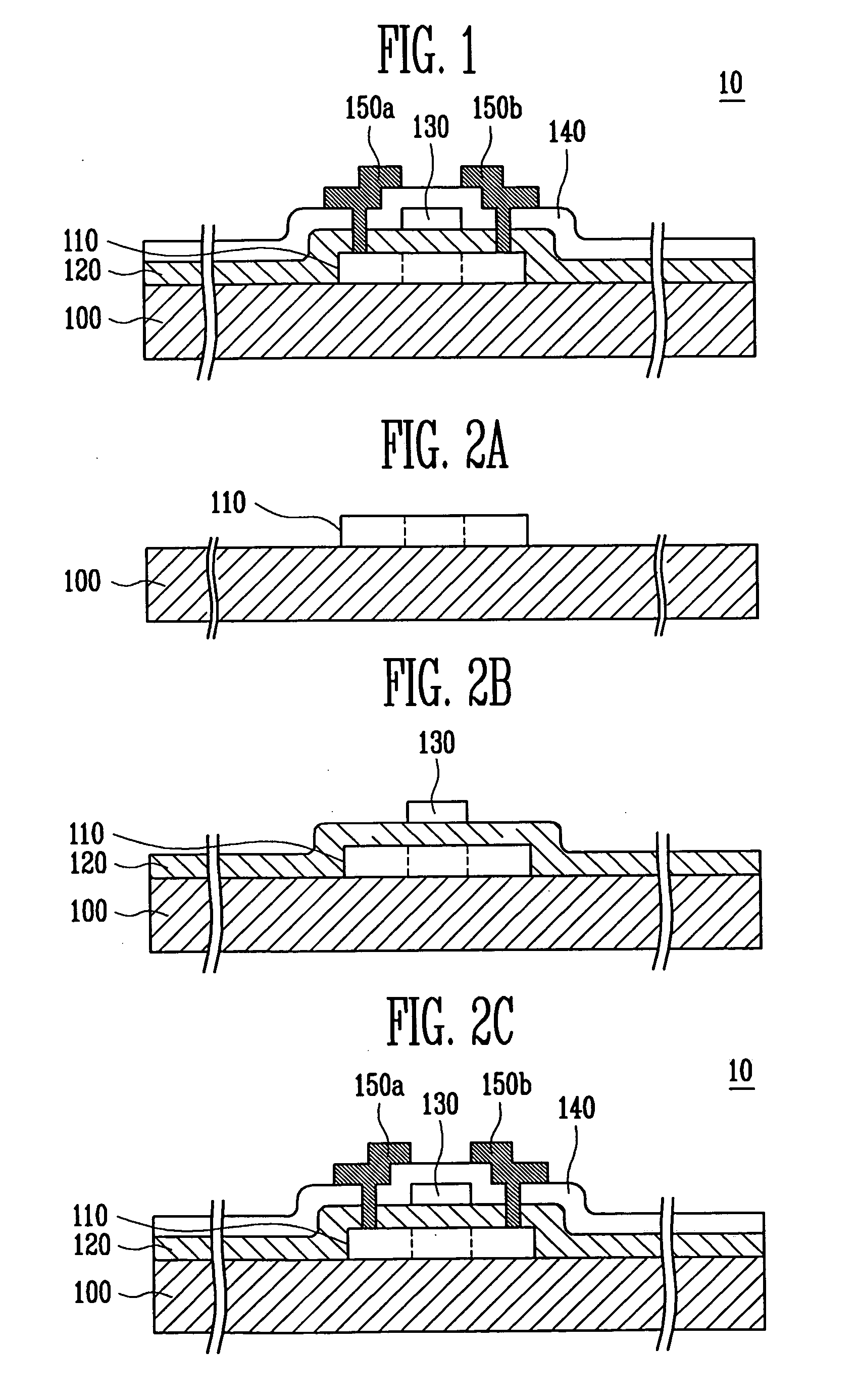
[0025]FIG. 1 is a schematic sectional view of a Transparent Thin Film Transistor (TFT) having a top gate structure according to the present invention.

[0026] Referring to FIG. 1, a transparent TFT 10 according to the first embodiment of the present invention includes a semiconductor layer 110 formed by coating a substrate 100 with a wide band gap semiconductor material whose band gap is no less than 3.0 eV to pattern the semiconductor material into a predetermined shape, an insulating layer 120 formed on the semiconductor layer 110, a gate electrode 130 formed on the gate insulating layer 120 to be patterned to correspond to the transparent semiconductor layer 110, an interlayer insulating layer 140 formed on the gate electrode 130, and source and drain electrodes 150a and 150b electrically connected to the transparent semiconductor layer 110 through contact holes (not shown) formed in the gate insulating layer 120 and the interlayer insulating layer 140.

[0027] The substrate 100 is ...

second embodiment

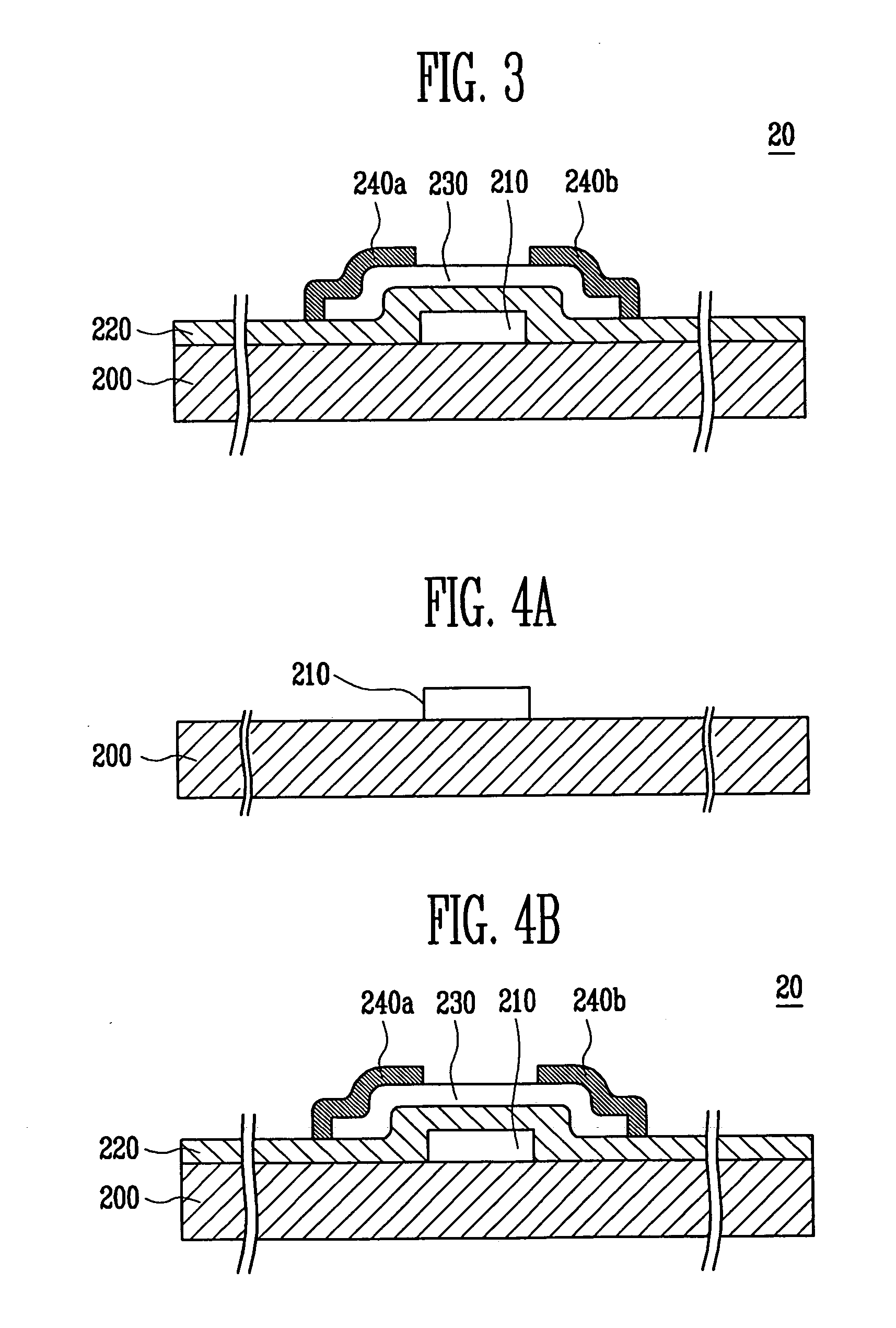
[0041]FIG. 3 is a schematic sectional view of a transparent TFT having a bottom gate structure according to the present invention.

[0042] Referring to FIG. 3, a transparent TFT 20 includes the gate electrode 210 formed on the substrate 200, the gate insulating layer 220 formed on the substrate 200 where the gate electrode 210 is formed, a transparent semiconductor layer 230 formed by coating the gate insulating layer 220 with an oxide, a nitride, or a carbide to pattern the applied material, and the source and drain electrodes 240a and 240b formed on the transparent semiconductor layer 230 so that the gate electrode 210 and a region of the transparent semiconductor layer 230 are exposed.

[0043] The substrate 200 is formed of an insulating material, such as glass, plastic, silicon, or a synthetic resin, and is preferably a transparent substrate, such as a glass substrate.

[0044] The gate electrode 210 is formed on the substrate 200 in a predetermined pattern and is formed of ITO, IZO,...


PUM


Abstract

A transparent thin film transistor (TFT) and its method of manufacture includes: a substrate, a transparent semiconductor layer formed by coating the substrate with an oxide, a nitride, or a carbide to pattern the material, a gate insulating layer formed on the transparent semiconductor layer, a gate electrode formed on the gate insulating layer to correspond to the transparent semiconductor layer, an interlayer insulating layer formed on the gate electrode, and source and drain electrodes electrically connected to the transparent semiconductor layer through contact holes formed in the interlayer insulating layer and the gate insulating layer.

Description

CLAIM OF PRIORITY [0001] This application makes reference to, incorporates the same herein, and claims all benefits accruing under 35 U.S.C.§ 119 from an application for TRANSPARENT THIN FILM TRANSISTOR AND FABRICATION METHOD FOR THE SAME earlier filed in the Korean Intellectual Property Office on the 14 Sep. 2005 and there duly assigned Serial No. 10-2005-0085897. BACKGROUND OF THE INVENTION [0002] 1. Field of the Invention [0003] The present invention relates to a transparent Thin Film Transistor (TFT) and its method of manufacture, and more particularly, to a transparent TFT in which a semiconductor layer is formed of a transparent material to improve its aperture ratio so that it is possible to relax design rules of a display and to improve the resolution of the display. [0004] 2. Discussion of Related Art [0005] Recently, a Thin Film Transistors (TFTs) have been widely used as switching devices to control pixels in display devices such as an Organic Light Emitting Displays (OLE...

Claims


Application Information

Patent Timeline
IPC IPC(8): H01L31/0312
CPCH01L29/7869H01L29/78681G02F1/136
Inventor JEONG, JAE KYEONGSHIN, HYUN SOOMO, YEON GON
Owner SAMSUNG MOBILE DISPLAY CO LTD
Why Eureka
Try Eureka