
Light emitting diode with diffraction lattice

a light-emitting diode and diffraction lattice technology, which is applied in the direction of basic electric elements, electrical equipment, semiconductor devices, etc., can solve the problems of low light extraction efficiency of ordinary leds, limited light extraction efficiency of led chips, and sensitive to emitted wavelengths, so as to improve light extraction efficiency and reduce the difference in the wavelength of led chips. , the effect of high efficiency

Inactive Publication Date: 2007-03-15
WANG PEI JIH +6
View PDF0 Cites 3 Cited by
  • Summary
  • Abstract
  • Description
  • Claims
  • Application Information

AI Technical Summary

Benefits of technology

"This patent describes a new LED technology that uses a special diffraction pattern to purify the color of the light emitted by the LED and increase its efficiency. This technology, called LED with a color purifying diffraction lattice (CPDL), uses a special pattern of tiny pores in a material called Al.sub.2O.sub.3 to filter the light emitted by the LED. This filtering improves the color purity of the LED and reduces the difference in wavelengths between different LED chips. The patent also describes a method for creating the CPDL pattern using anodic oxidation on an Al film. Overall, this technology can enhance the performance and quality of LED lighting."

Problems solved by technology

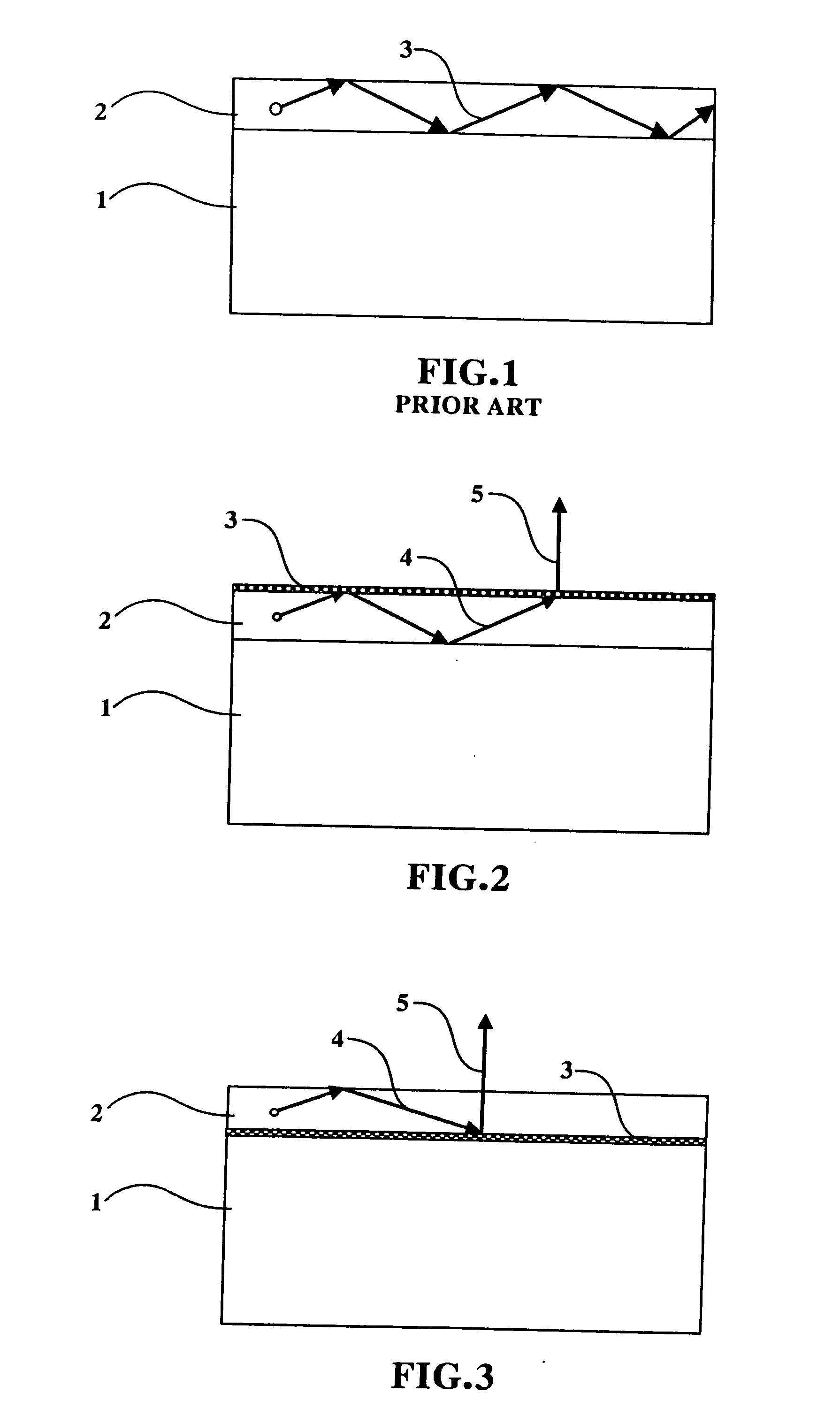
Generally light extraction efficiency of LEDs is limited by high refractive index of the LED chip material which prevents the light escape from the LED chip when its incident angles is higher than the angle of total internal reflection FIG. 1.
This results in low light extraction efficiency of ordinary LEDs which is typically less than 10%.
All above methods allow to suppress the light reflection at the surface of the LED chip and change the angular bandwidth of light which may transmit power into the ambient, but they are not very sensitive to the emitted wavelength.
This does not allow a precise fitting the light extraction properties to a given wavelength and filtering of the light spectrum emitted by the LED.

Method used


Image

  • Light emitting diode with diffraction lattice
  • Light emitting diode with diffraction lattice
  • Light emitting diode with diffraction lattice

Examples


example 1

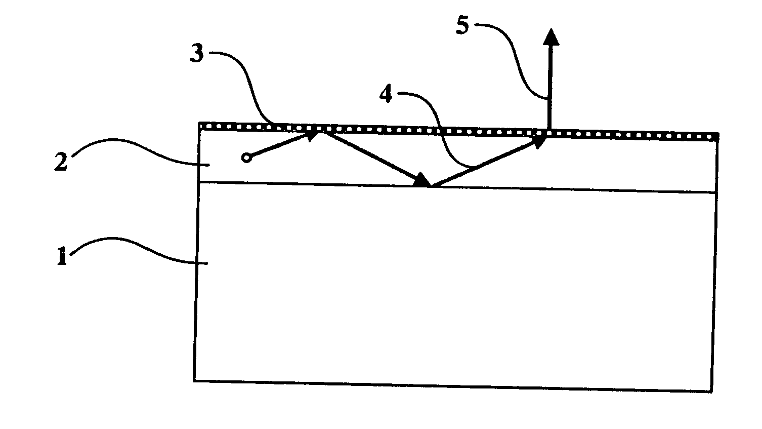
[0023] The principal scheme of the LED embodied in Example 1 is shown in FIG. 2. It has a sapphire (Al.sub.2O.sub.3) substrate 1 upon which a gallium-nitride-based LED structure 2 is grown.

[0024] On the gallium-nitride-based LED structure a two-dimensional CPDL 3 is formed by dry surface etching. The light scattering by CPDL convert the laterally propagating light 4 into the vertically propagating light 5 and, thus, enhance the light extraction efficiency.

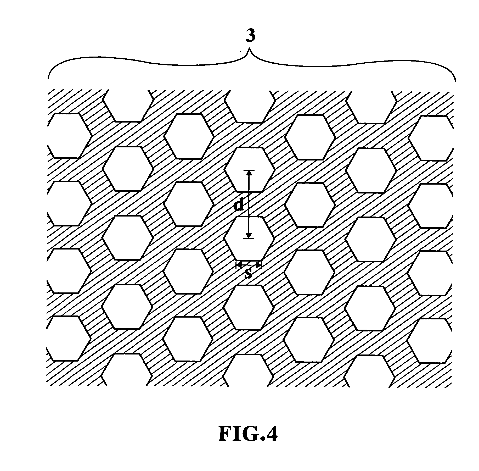
[0025] The CPDL structure is shown in FIG. 4.

[0026] The period d of the CPDL should satisfy the equation d=m.lamda. / n, where m=1, 2, 3 . . . and .lamda. is the wavelength of the light generated by LED, and n is the refraction index of GaN. To make the scattering with m=1, 2, 3 . . . most effective the zero order of diffraction with m=0 should be suppressed. This happens when height of the hexagonal islands forming CPDL is h=.lamda.(2l+1) / 2n, l=0, 1, 2, 3 . . ., and total areas of islands and trenches in CPDL are equal. To make t...

example 2

[0028] The principal scheme of the LED embodied in Example 2 is shown in FIG. 3. It has a sapphire (Al.sub.2O.sub.3) substrate 1 on which a two-dimensional CPDL 3 is formed by surface etching. On the CPDL a gallium-nitride-based LED structure 2 is grown.

[0029] The CPDL structure is shown in FIG. 5.

[0030] The light scattering by CPDL convert the laterally propagating light 4 into the vertically propagating light 5 and, thus, enhance the light extraction efficiency.

[0031] The period d of the CPDL should satisfy the equation d=m.lamda. / n, where m=1, 2, 3 . . . and .lamda. is the wavelength of the light generated by LED, and n is the refraction index of GaN. To make the scattering with m=1, 2, 3 . . . most effective the zero order of diffraction with m=0 should be suppressed. This happens when heights of the hexagonal islands forming CPDL is h=.lamda.(2l+1)2n, l=0, 1, 2, 3 . . , and total areas of islands and trenches in CPDL are equal. To make these areas equal the side s hexagon is...

example 3

[0035] The principal scheme of the LED embodied in Example 3 is shown in FIG. 2. It has a sapphire (Al.sub.2O.sub.3) substrate 1 upon which a gallium-nitride-based LED structure 2 is grown.

[0036] On the gallium-nitride-based LED structure a two-dimensional Al.sub.2O.sub.3 CPDL 3 is deposited.

[0037] The Al.sub.2O.sub.3 CPDL 3 is formed by an anodic oxidation of Al film.

[0038] The CPDL structure is shown in FIG. 6.

[0039] The period d of the CPDL should satisfy the equation d=m.lamda. / n, where m=1, 2, 3 . . . and .lamda. is the wavelength of the light generated by LED, and n is the refraction index of GaN. To make the scattering with m=1, 2, 3 . . . most effective the zero order of diffraction with m=0 should be suppressed. This happens when depths of the cylindrical holes forming CPDL is h=.lamda.(2l+1) / 2n, l is a positive integer number or zero, and their radii r satisfy the equation r=d(3 / 4.pi.).sup. 1 / 2.

[0040] For LED with .lamda.=0.5 .mu.m the parameters of the CPDL with m=1,...


PUM


Abstract

A method of fabricating light emitting diodes (LED) with a colour purifying diffraction lattice (CPDL) is suggested, the essence of the invention is in the use of the coherent scattering of the light by the CPDL for colour purifying of the light emitted by the LED and enhancement its extraction efficiency, the CPDL is a hexagonal two-dimensional periodical pattern on the surface of the LED structure or an internal interface resulting in the periodical variation in the refractive index with the period d The period of CPDL satisfies the equation d=m.lamda. / n, where m is a positive integer number, .lamda. is the wavelength of the light generated by LED, and n is the refraction index of LED structure. The height of the hexagonal islands forming CPDL is h=.lamda.(2l+1) / 2n, l is a positive integer number or zero. Use of CPDL allows to convert the laterally propagating light into the vertically propagating and simultaneously filter its spectrum.

Description

RELATED APPLICATIONS [0001] This application is a Divisional patent application of co-pending application Ser. No. 10 / 928,094, filed on 30 Aug. 2004.BACKGROUND OF THE INVENTION [0002] 1. Field of the Invention [0003] The present invention relates to a method for fabricating a light emitting diodes (LED). More particularly, the invention relates to a method of fabricating LED with pure colour and enhanced light extraction efficiency. [0004] 2. Description of the Prior Art [0005] Generally light extraction efficiency of LEDs is limited by high refractive index of the LED chip material which prevents the light escape from the LED chip when its incident angles is higher than the angle of total internal reflection FIG. 1. This results in low light extraction efficiency of ordinary LEDs which is typically less than 10%. [0006] To enhance the light extraction efficiency various methods had been proposed. [0007] These are pyramidal-like shaped LED chip taught by M. R. Krames et. al. Applied...

Claims


Application Information

Patent Timeline
Patent Type & Authority Applications(United States)
IPC IPC(8): H01L33/00H01L33/20H01L33/46
CPCH01L33/20H01L2933/0083H01L33/46
Inventor WANG, PEI-JIHCHANG, PAN-TZUHUANG, WEN-CHIEHWANG, JAMESSHRETER, YURY GEORGIEVICHREBANE, YURY TOOMASOVICHGORBUNOV, RUSLAN IVANOVICH
Owner WANG PEI JIH
Learn More