

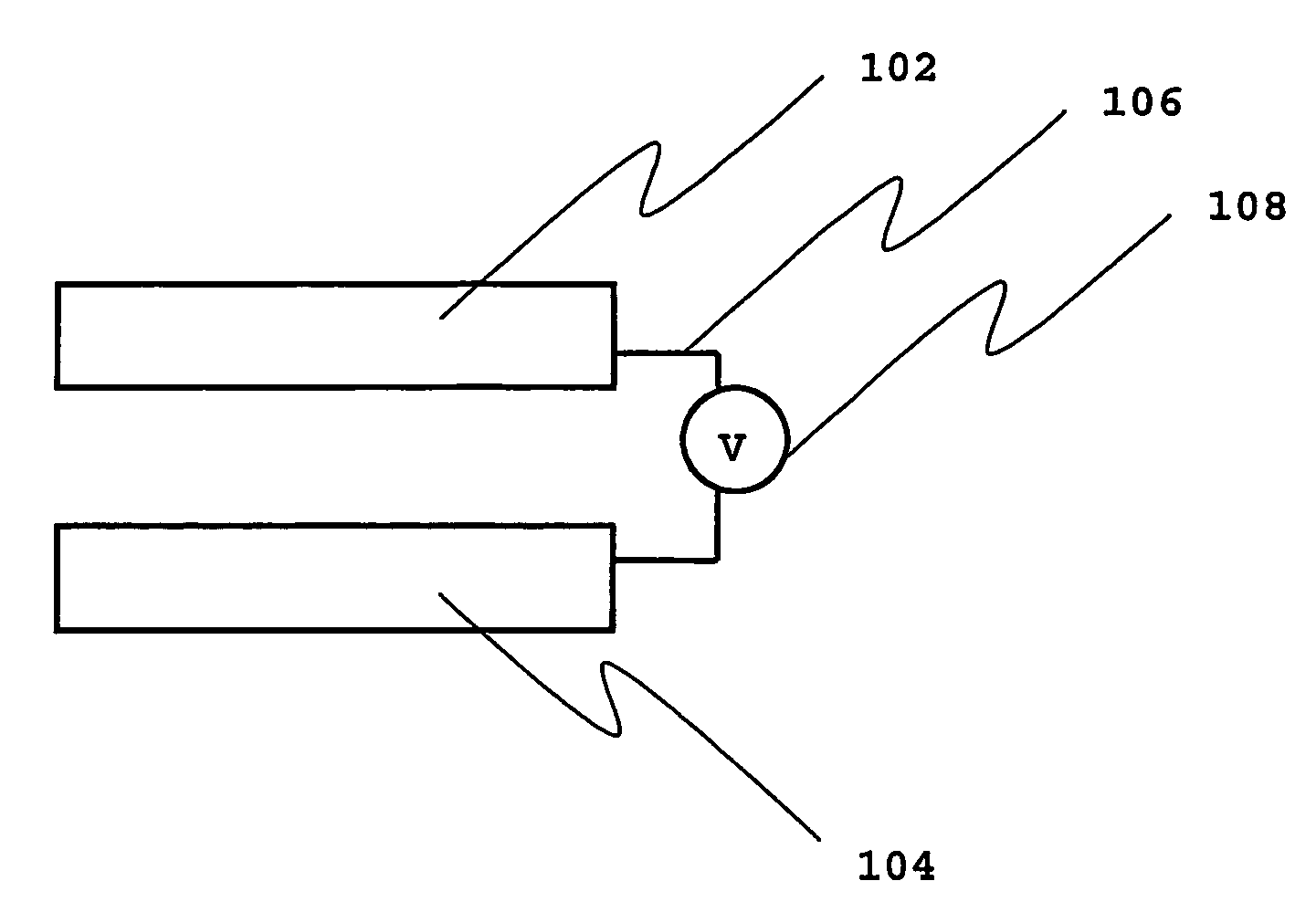
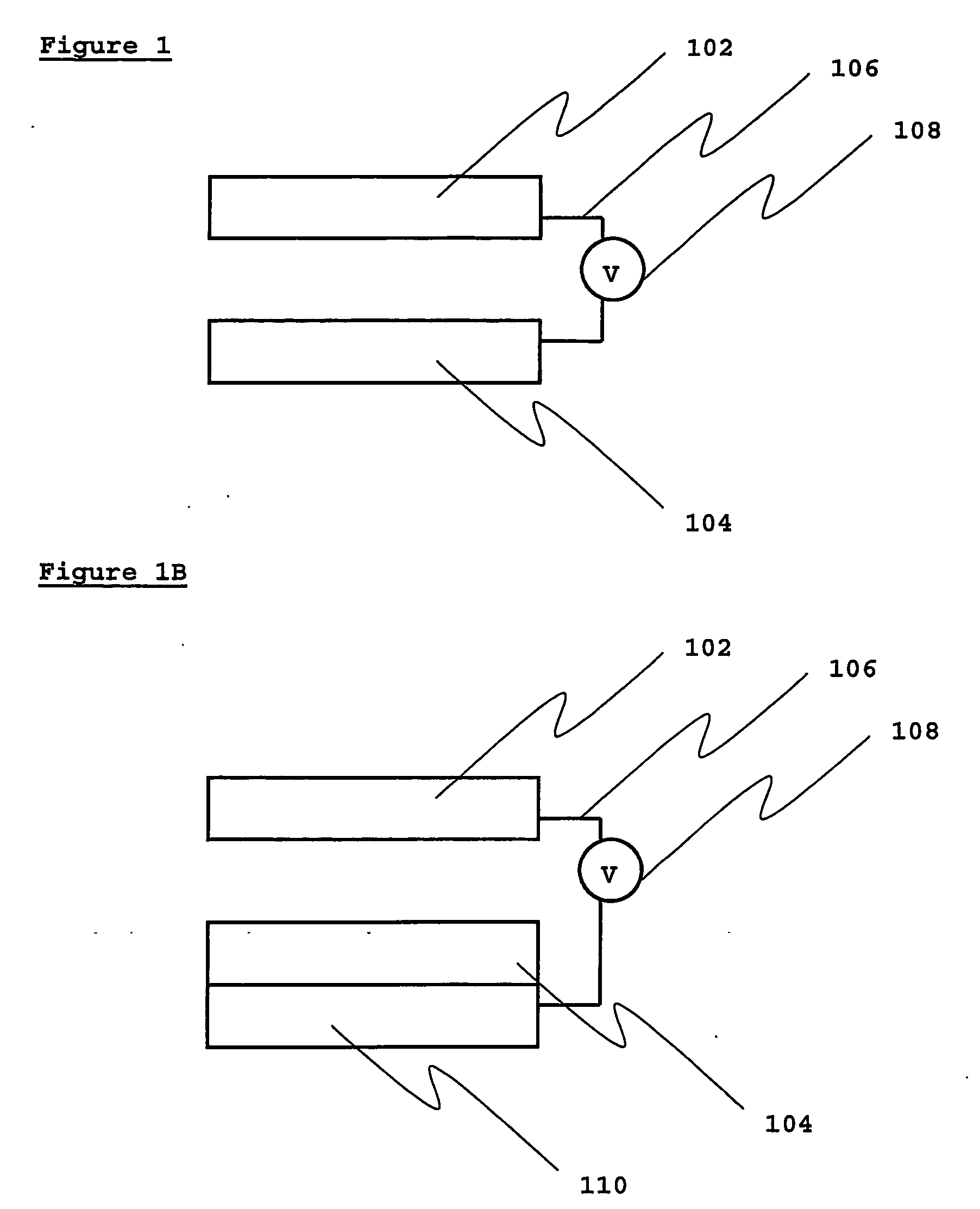
Tunneling gap diodes
a technology of gap diodes and tunnel diodes, which is applied in the direction of diodes, semiconductor devices, electrical apparatus, etc., can solve the problems of imposing additional technological difficulties, 1% or less, and insufficient material availability, etc., to achieve the effect of increasing the efficiency of heat pumping or power generation, increasing energy, and increasing the efficiency of tunnel diodes
- Summary
- Abstract
- Description
- Claims
- Application Information
AI Technical Summary
Benefits of technology
Problems solved by technology
Method used
Image

Examples
example
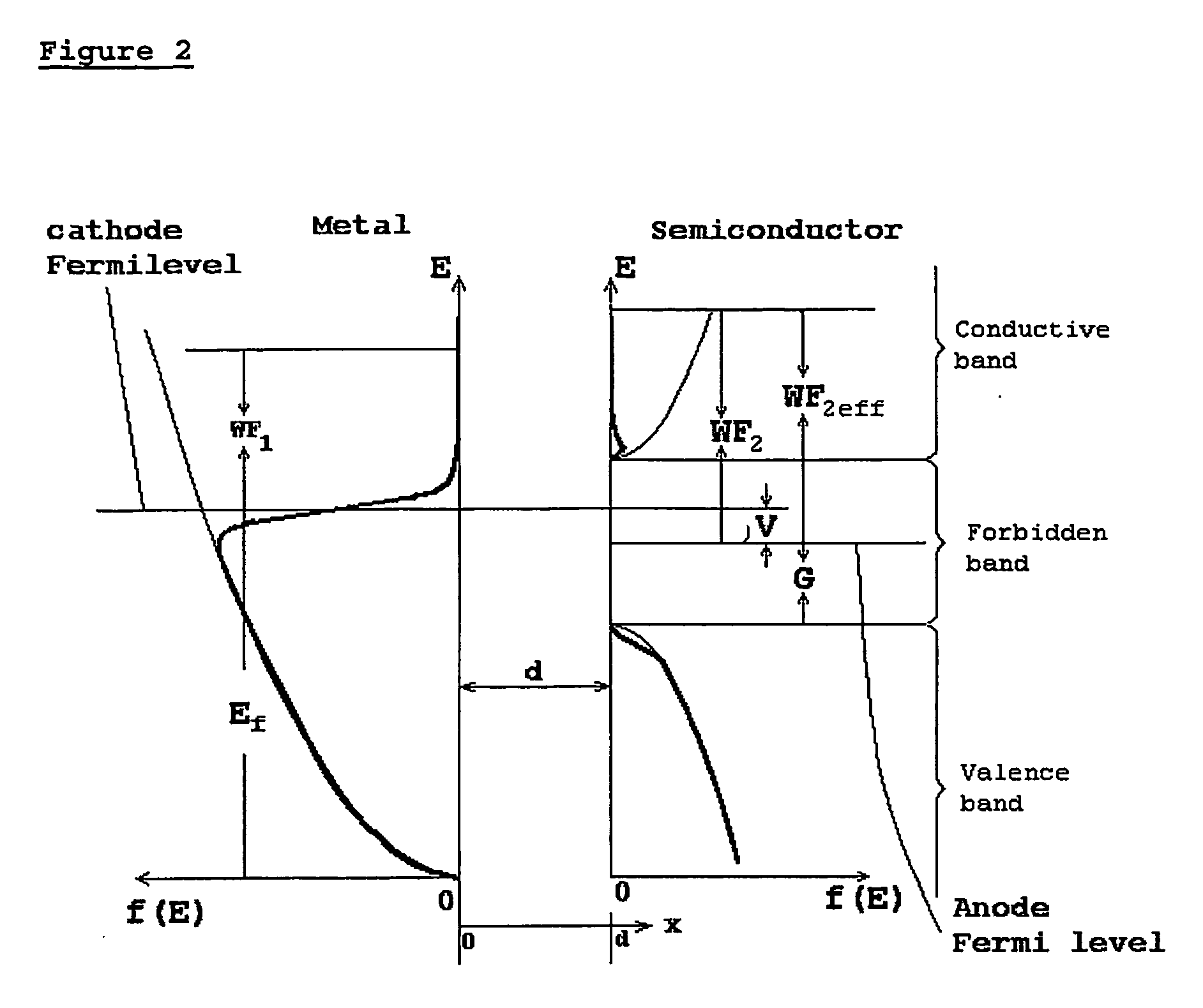
[0032] In one embodiment, pure Ge is the semiconductor. It has G=0.75 eV, and G / 2=0.375 eV, a little more than optimum WF for thermionic diode for Tc=300 K (˜0.33 eV). Even at room temperature, Ge has electron concentration in conductive band ˜1013 cm−3, which is sufficient for electrical conductivity for thin layer. If it is assumed that electrodes are treated by Cs and O2 and has WF1=WF2=1 eV, then the output parameters for cooling with d=2.5 nm, Tc=300 K, Th=350 K are given below:
j,Qc,W,hcool / hcoolV, VA / cm2W / cm2W / cm2COPhcoolCarnot0.101.760.630.1773.560.780.91 0.146.822.220.7962.32 0.6990.8160.2036.69.707.3151.320.570.665
Here j is resulting diode current, Qc cooling power, W = j*V = spent power.
[0033] Calculations were fulfilled with some simplifications as follows.
[0034] For elementary tunnel current from emitter, which is produced by electrons of the metal conductive band with energy interval E, E+dE and with energy Ex, Ex+dEx in direction normal to the emitted surface, we u...
PUM
 Abstract
Description
Claims
Application Information