Display device and drive method of same

Inactive Publication Date: 2007-03-15
JAPAN DISPLAY WEST
View PDF8 Cites 49 Cited by
  • Summary
  • Abstract
  • Description
  • Claims
  • Application Information

AI Technical Summary

Benefits of technology

[0035] According to the present invention, there is the advantage that both of the black luminance and t

Problems solved by technology

However, when employing the capacity coupling drive unit described in Japanese Patent Publication (A) No. 2-157815 for a liquid crystal display device using a liquid crystal material having the characteristic of the liquid crystal dielectric constant ε for the applied voltage such as shown in FIG. 3 (for normally white specifications), there is the drawback of the white luminance becoming black (dropping) when trying to optimize the black luminance as shown in the following equation (1), FIG. 4, and FIG. 5.
Due to this, in current liquid crystal display devices employing the capacity coupling drive unit, there is the drawback of not being able to simultaneously optimize the black luminance and the white luminance.
Further, when employing this capacity coupli

Method used


Image

  • Display device and drive method of same
  • Display device and drive method of same
  • Display device and drive method of same

Examples


first embodiment

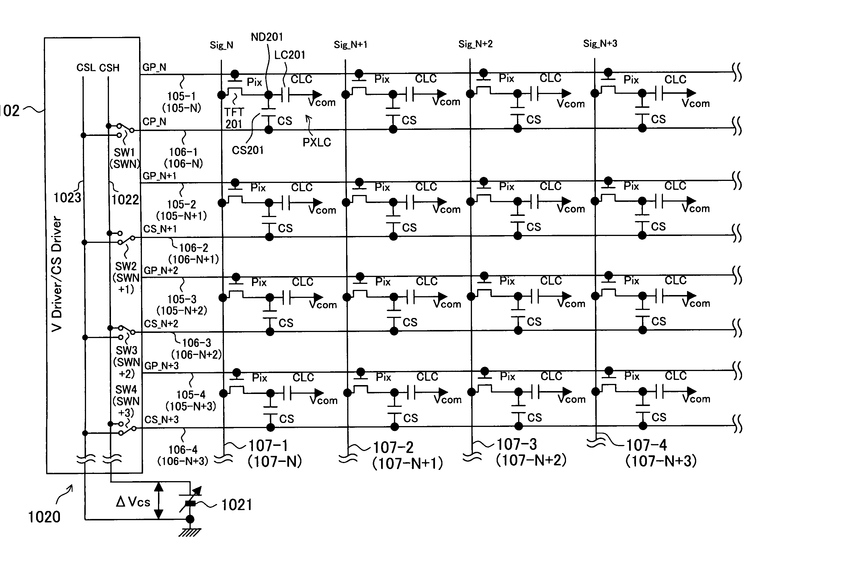
[0071]FIG. 6 is a figure showing an example of the configuration of an active matrix type display device according to a first embodiment of the present invention using for example liquid crystal cells as display elements of pixels (electrooptic elements).

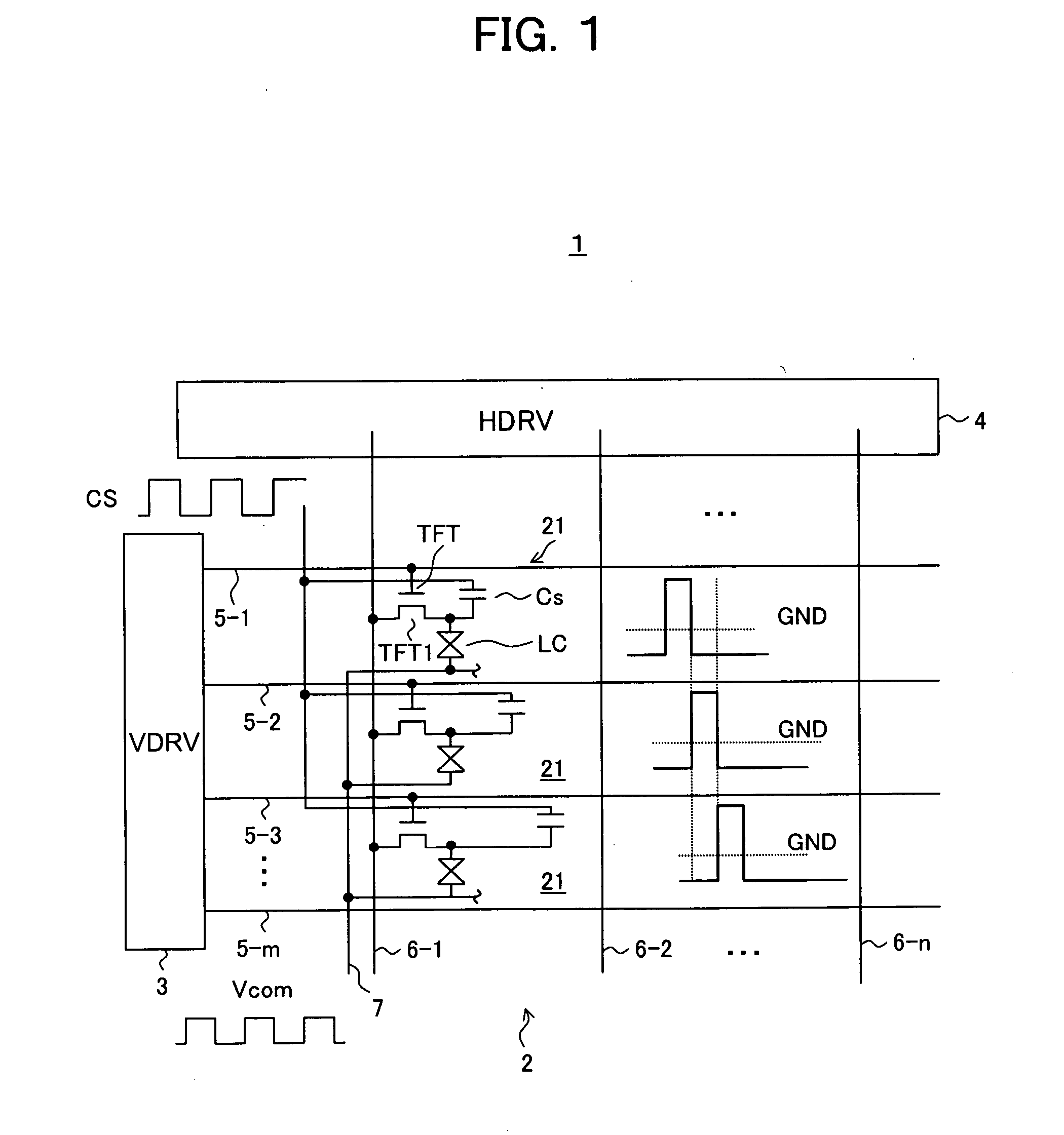
[0072] The display device 100 has as its main constituent elements an effective pixel section 101, a vertical drive circuit (VDRV) 102, a horizontal drive circuit (HDRV) 103, and a common voltage generation circuit (VcomGen) 104.

[0073] The effective pixel section 101, as shown in FIG. 7, is comprised of a plurality of pixel circuits PXLC arrayed in an m×n matrix. Specifically, to enable normal display overall, for example, 320×RGB×320 number of pixel circuits are arrayed. Note that in FIG. 7, for simplification of the figure, this is shown as a 4×4 matrix array.

[0074] Each pixel circuit PXLC, for example, as shown in FIG. 7, is configured by a TFT (thin film transistor) 201 as a switching element, a liquid crystal cell LC201 with...

second embodiment

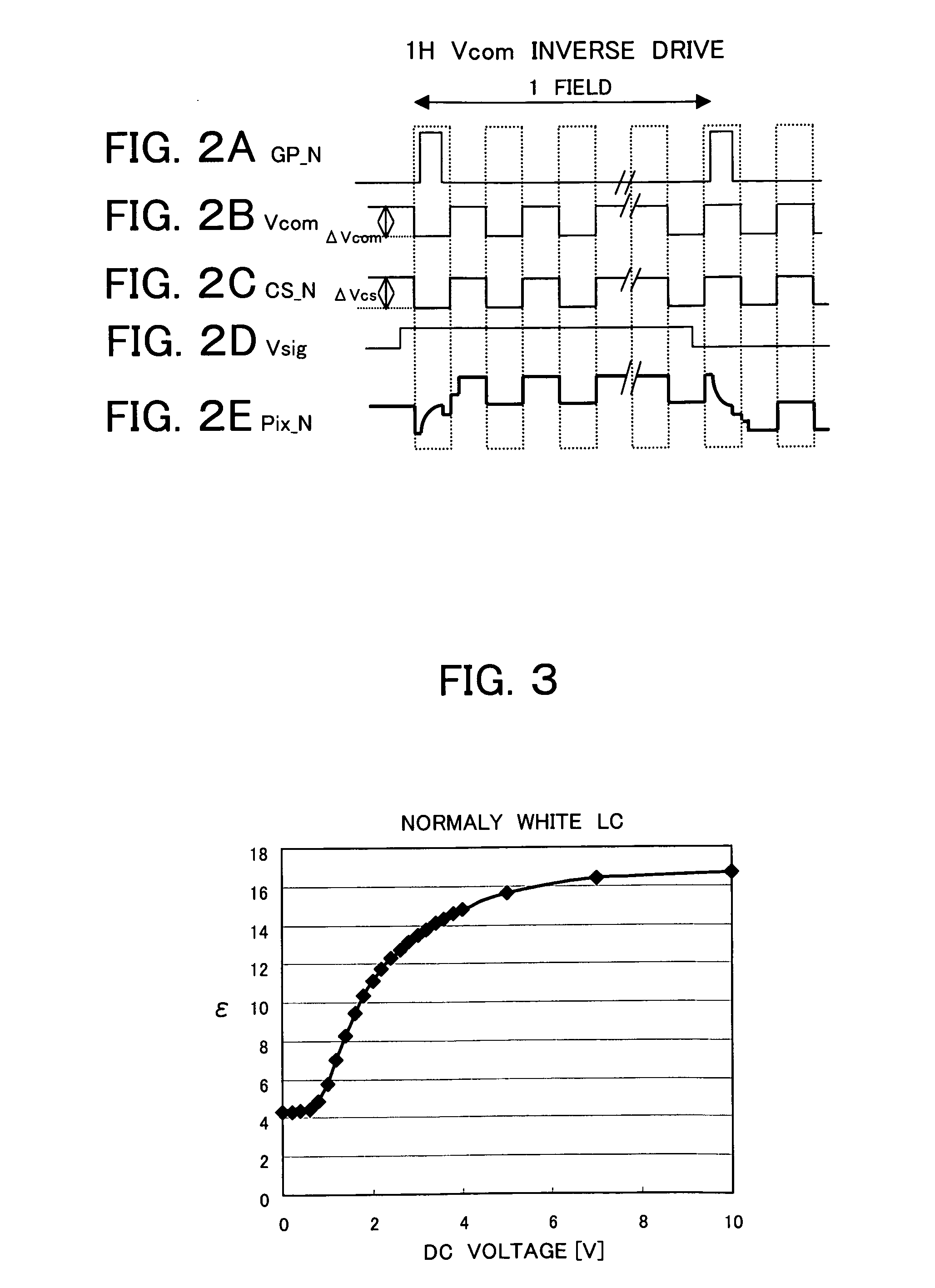
[0117] Next, one feature of the present invention, that is, the correction of the storage signal CS by the correction circuit 109 shown in FIG. 6 so as to optimize the optical characteristics so that the pixel potential detected from the detection area 108 comprised of the dummy pixel section (monitor section) becomes any desired potential will be explained by a specific example of the configuration.

[0118] In the present embodiment, fluctuations in the dielectric constant of the liquid crystals due to changes in the drive temperature and fluctuations in the thickness of the insulating film forming the storage capacitor CS201 and fluctuations in the liquid crystal cell cap due to fluctuations in mass production cause the voltage applied to the liquid crystals to fluctuate. This amount of fluctuation is detected electrically. The fluctuations in the voltage applied to the liquid crystals are suppressed in order to suppress changes due to the temperature of the display or variations a...


PUM


Abstract

A display device having a pixel section including a plurality of pixel circuits arrayed in a matrix, a plurality of scan lines, a plurality of capacity lines, a plurality of signal lines, a drive circuit, and a generation circuit generating a small amplitude common voltage signal switching in level at a predetermined cycle, wherein each pixel circuit arranged at the pixel section contains a display element having a first pixel electrode and a second pixel electrode and a storage capacitor having a first electrode and a second electrode, the first pixel electrode of the display element, the first electrode of the storage capacitor, and one terminal of the switching element are connected, the second electrode of the storage capacitor is connected to the capacity lines arrayed in a corresponding row, and the common voltage signal is applied in a second pixel electrode of the display element.

Description

CROSS REFERENCE TO RELATED APPLICATION [0001] The present invention contains subject matter related to Japanese Patent Application No. 2005-237924 filed in the Japan Patent Office on Aug. 18, 2005, and Japanese Patent Application No. 2005-248104 filed in the Japan Patent Office on Aug. 29, 2005 the entire contents of which being incorporated herein by reference. BACKGROUND OF THE INVENTION [0002] 1. Field of the Invention [0003] The present invention relates to an active matrix-type display device comprised of liquid crystal cells or other display elements of pixels (electrooptic elements) arrayed in a display region in a matrix and a method of driving the same. [0004] 2. Description of the Related Art [0005] Display devices, for example, liquid crystal display devices using liquid crystal cells for the display elements of the pixels (electrooptic elements), feature thin profiles and low power consumptions. Utilizing these features, they are being used in, for example, personal digi...

Claims


Application Information

Patent Timeline
IPC IPC(8): G09G3/36
CPCG09G3/3614G09G3/3655G09G3/3659G09G2320/029G09G2310/06G09G2320/0238G09G2300/0876G02F1/133G09G3/20G09G3/36
Inventor ITAKURA, NAOYUKIFUKANO, TOMOYUKINAKAJIMA, YOSHIHARUSATO, TOMOHIKOTAKEUCHI, TAKEYA
Owner JAPAN DISPLAY WEST
Why Eureka
Try Eureka