Lithographic apparatus and device manufacturing method
- Summary
- Abstract
- Description
- Claims
- Application Information
AI Technical Summary
Benefits of technology
Problems solved by technology
Method used
Image

Examples
Embodiment Construction
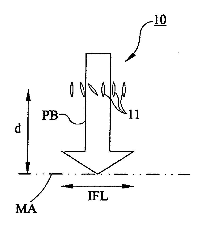
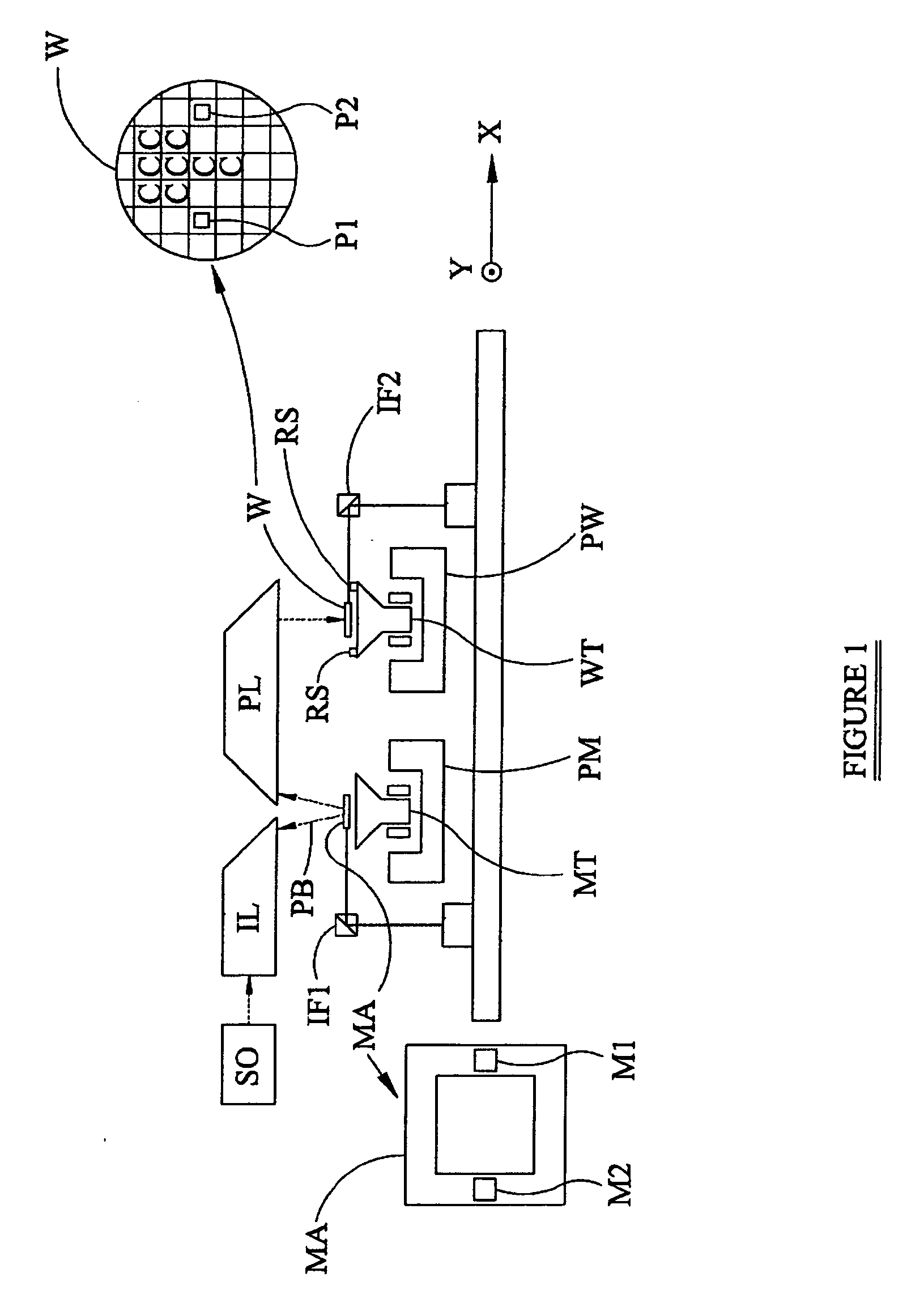
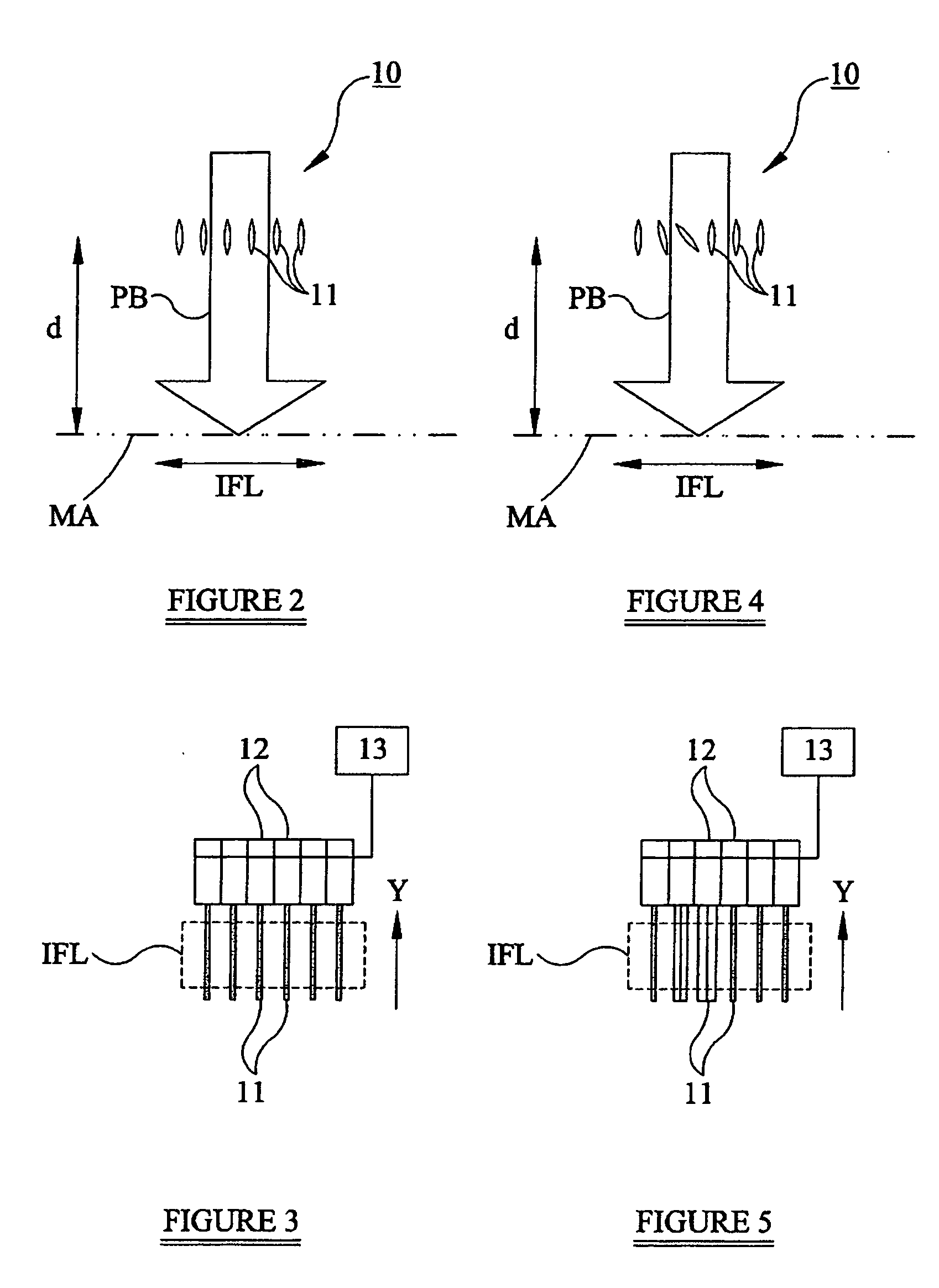
[0036]FIG. 1 schematically depicts an example of a lithographic apparatus intended to be used with DUV radiation having a wavelength of less than 200 nm. In each case the apparatus includes: [0037] an illumination system (illuminator) IL for providing a projection beam PB of radiation (e.g. UV radiation). [0038] a support structure (e.g. a mask table) MT for supporting patterning means (e.g. a mask) MA and connected to first positioning means PM for accurately positioning the patterning means with respect to item PL; [0039] a substrate table (e.g. a wafer table) WT for holding a substrate (e.g. a resist-coated wafer) W and connected to second positioning means PW for accurately positioning the substrate with respect to item PL; and [0040] a projection system (e.g. a refractive or reflective projection lens) PL for imaging a pattern imparted to the projection beam PB by patterning means MA onto a target portion C (e.g. comprising one or more dies) of the substrate W.
[0041] The illum...
PUM
 Abstract
Description
Claims
Application Information