Interface circuit

a technology of interface circuits and circuits, applied in the field of interface circuits, can solve the problems of circuits that are not so used, inaccurate data receipt by memory controllers, and inability to accurately execute arbitrations, etc., and achieve the effects of reducing power consumption, improving circuit measurement accuracy, and easy grasping

Inactive Publication Date: 2007-03-15
RENESAS ELECTRONICS CORP
View PDF10 Cites 55 Cited by
  • Summary
  • Abstract
  • Description
  • Claims
  • Application Information

AI Technical Summary

Benefits of technology

[0024] According to the interface circuit of the present invention, an appropriate one of the first synchronizing circuit and the second synchronizing circuit can be designated based on a preset value, making it possible to easily grasp which one of the synchronizing circuits is used. Based on the above, an unused one of the synchronizing circuits is put into a suspend mode, whereby power consumption can be reduced more than the conventional interface circuit.
[0025] Further, the used synchronizing circuit can be switched by a delay determination setting circuit, so a circuit measurement precision can be improved upon the delivery inspection or other such testing. Thus, the circuit can be more accurately tested, so a reliability of the interface circuit can be improved.
[0026] Furthermore, a delay of strobe signal relative to the reference clock is measured by the delay determining circuit, and the synchronizing circuit to be used can be determined based on the measurement result. Thus, even if signals that are largely different in delay time with respect to the reference clock are input, the signals can be accurately synchronized with the reference clock.

Problems solved by technology

However, the memory controller 112 cannot accurately receive the data unless the data is synchronized with the system clock sysCLK.
The interface circuit 113 of the Related Art 1 has a problem in that arbitration cannot be accurately executed depending on a delay of the strobe signal with respect to the system clock sysCLK.
That is, the interface circuit 213 of the Related Art 2 has a problem that the two synchronizing paths are being active all the time, so a circuit that is not so used consumes considerable power, and power consumption increases more than necessary.
Further, the interface circuit 213 of the Related Art 2 dynamically switches the synchronizing paths, so it is difficult to detect which synchronizing path is tested upon the circuit functional test for delivery inspection.
That is, it is difficult to test the interface circuit 213 with reliability.

Method used


Image

  • Interface circuit
  • Interface circuit
  • Interface circuit

Examples


first embodiment

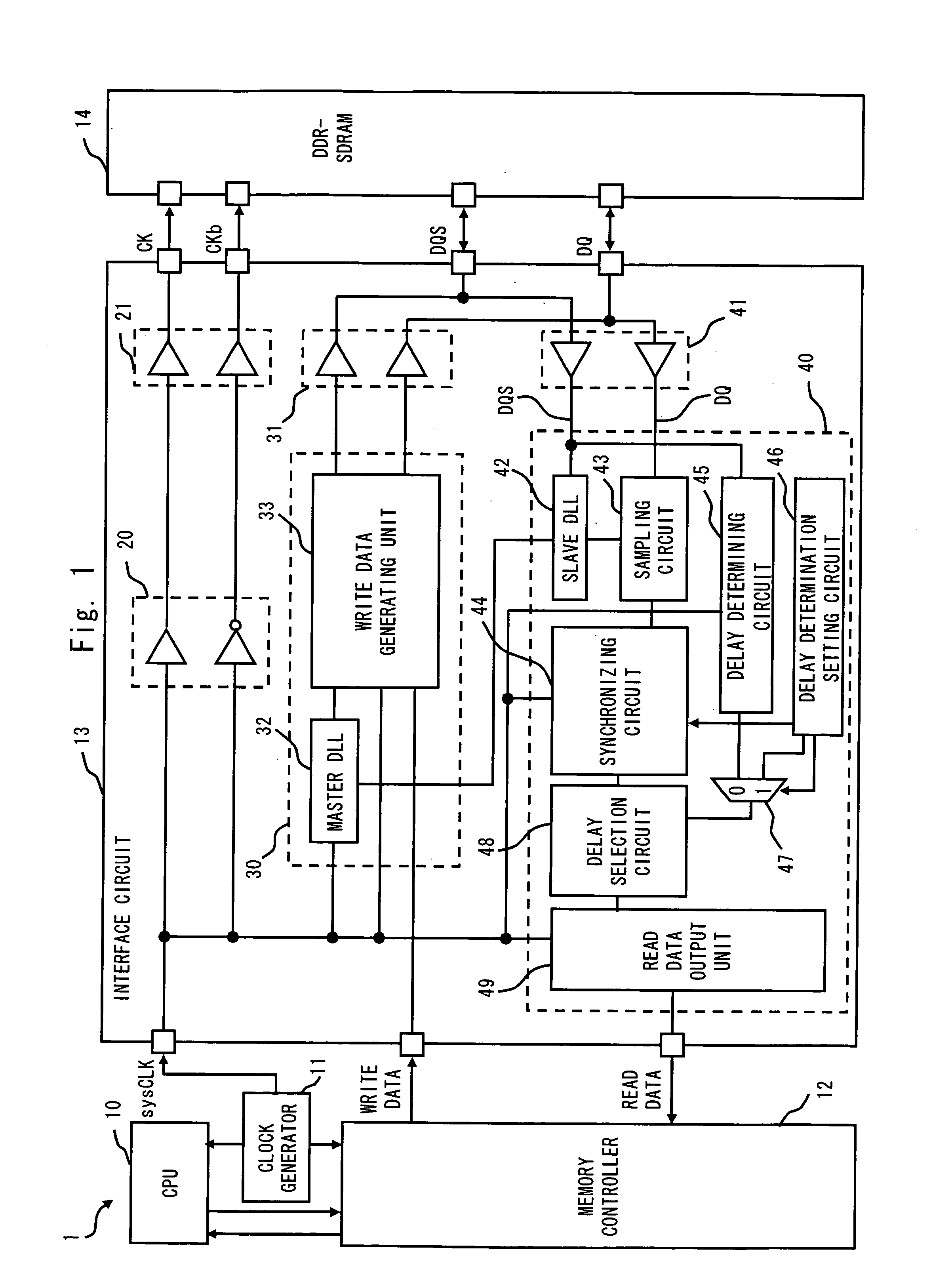
[0037]FIG. 1 is a block diagram showing a data processing system 1 including an interface circuit according to a first embodiment of the present invention. As shown in FIG. 1, the system 1 includes a CPU 10, a clock generator 11, a memory controller 12, an interface circuit 13, and a DDR-SDRAM 14. In the system 1, for example, the CPU 10, the clock generator 11, the memory controller 12, and the interface circuit 13 are mounted onto the same semiconductor substrate, and the DDR-SDRAM 14 is mounted onto a different semiconductor substrate.

[0038] Each block of the data processing system 1 operates in response to a reference clock (for example, system clock sysCLK) generated by the clock generator 11. The CPU 10 processes data based on a command of an application stored in a storage device or the like (not shown). Further, the CPU 10 transmits / receives data to / from the memory controller 12 and to / from the DDR-SDRAM 14 through the interface circuit 13 as needed. The memory controller 1...

second embodiment

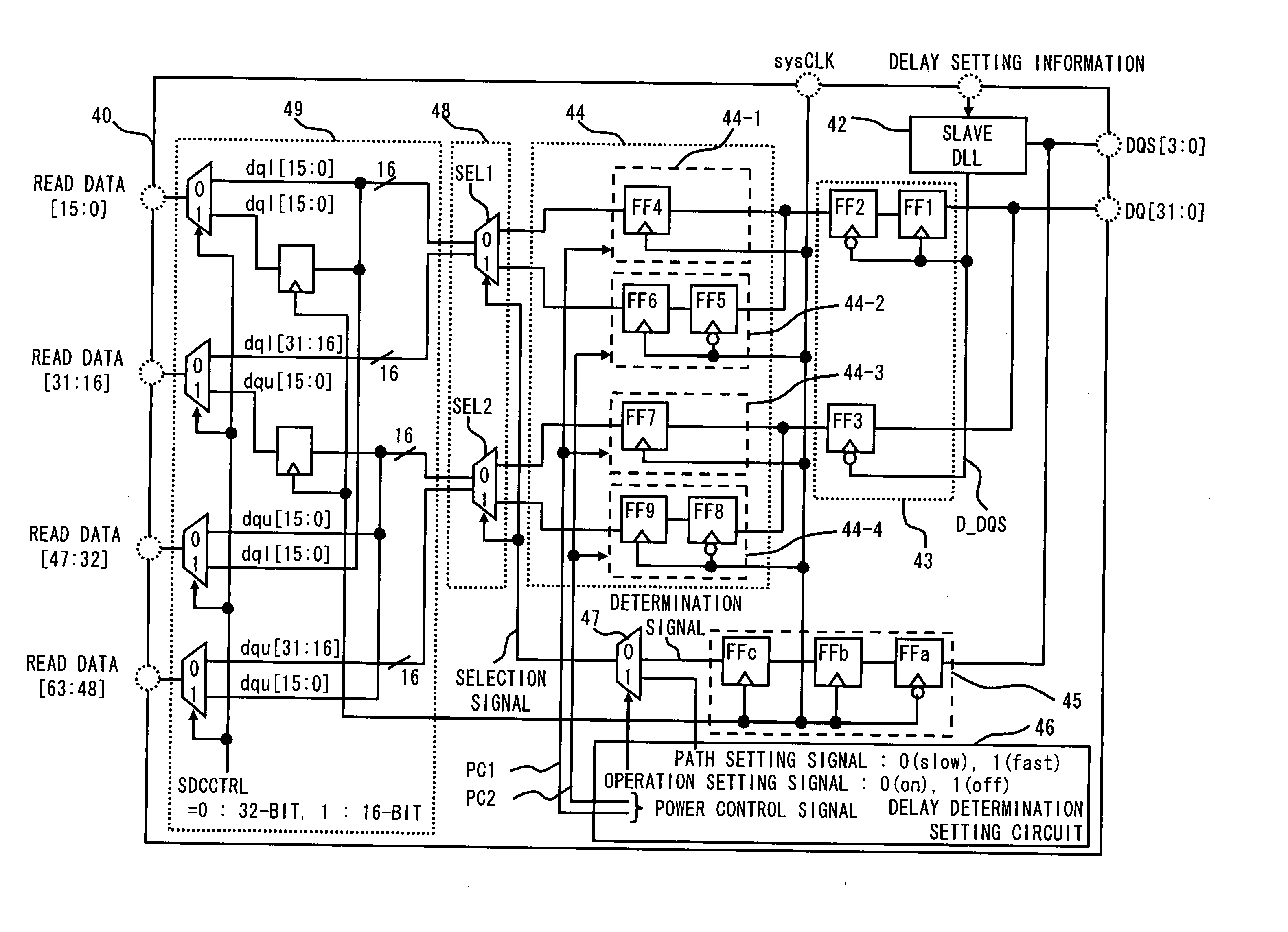
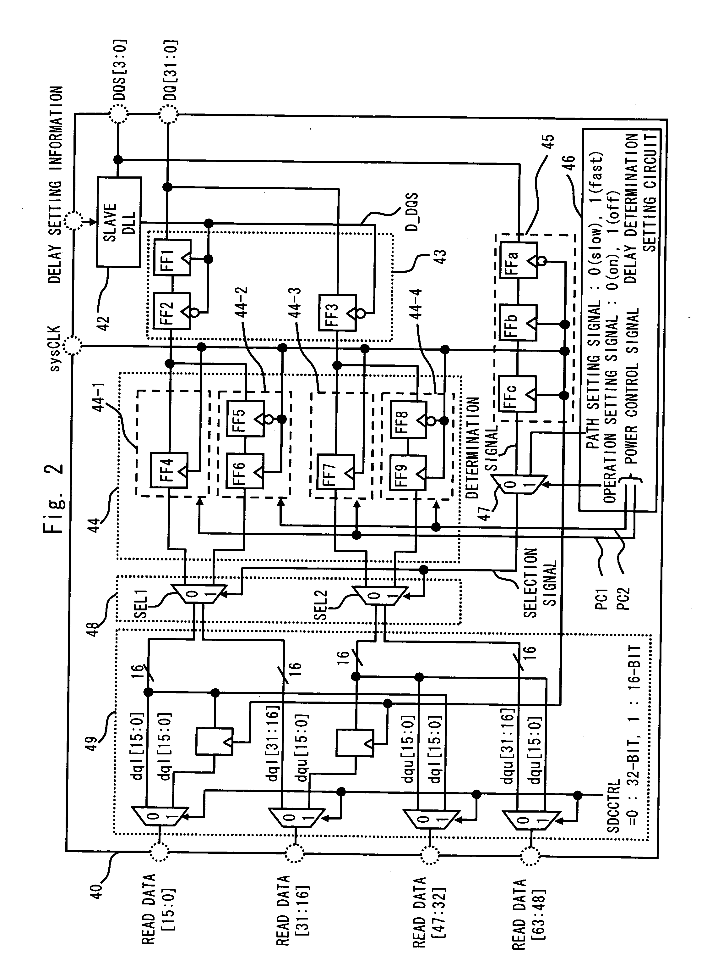
[0085]FIG. 5 shows a read data synchronizing unit 50 of an interface circuit according to a second embodiment of the present invention. The read data synchronizing unit 50 of the second embodiment is substantially the same circuit as the read data synchronizing unit 40 of the first embodiment. The read data synchronizing unit 40 of the first embodiment switches the static selection and the dynamic selection of a path of the synchronizing circuit 44 by means of the selector 47. In contrast, the read data synchronizing unit 50 of the second embodiment is structured such that the determination signal of the delay determining circuit 45 is input to the delay determination setting circuit 51, and the delay determination setting circuit 51 outputs a selection signal for selecting a path of the synchronizing circuit 44. The same components as those of the read data synchronizing unit 40 of the first embodiment are denoted by identical reference numerals, and description thereof is omitted ...


PUM


Abstract

An interface circuit includes: a first synchronizing circuit for synchronizing a signal having a delay equal to or more than a predetermined period with respect to a reference clock, with the reference clock; a second synchronizing circuit for synchronizing a signal having a delay less than the predetermined period with respect to the reference clock, with the reference clock; a delay determining circuit for outputting a determination signal based on a delay of the signal relative to the reference clock; a delay determination setting circuit for outputting a path setting signal that designates an output value of one of the first synchronizing circuit and the second synchronizing circuit based on a preset value; and a delay selecting circuit for selecting and outputting an output value of one of the first synchronizing circuit and the second synchronizing circuit based on one of the determination signal and the path setting signal.

Description

BACKGROUND OF THE INVENTION [0001] 1. Field of the Invention [0002] The present invention relates to an interface circuit, and more particularly to an interface circuit that sends data, which has been applied to a block not in sync with a system clock, toward another block in sync with the system clock. [0003] 2. Description of Related Art [0004] In the case of configuring a system using plural functional circuits, there is a possibility that the functional circuits receive / transmit data not synchronized with a system clock. In such a case, it is necessary to provide an interface circuit including a synchronizing circuit for synchronizing the data asynchronous with the system clock with the system clock. As an example of the interface circuit, there is an interface circuit provided between a mobile DDR-SDRAM (Double Data Rate-Synchronous Dynamic Random Access Memory) and a memory controller. FIG. 6 is a block diagram showing a data processing system 100 including an interface circui...

Claims


Application Information

Patent Timeline
Patent Type & Authority Applications(United States)
IPC IPC(8): G11C8/00
CPCG11C7/1051G11C7/1066G11C7/22G11C29/50012G11C29/02G11C29/022G11C29/028G11C7/222
Inventor MURAYAMA, TOHRU
Owner RENESAS ELECTRONICS CORP
Why Eureka
Try Eureka