
Programming method of non-volatile memory device having multi-plane structure

a non-volatile memory and multi-plane technology, applied in the direction of memory architecture accessing/allocation, instruments, computing, etc., can solve the problems of reducing program performance and conventional program method requiring a significantly longer program time, and achieve the effect of reducing program tim

Inactive Publication Date: 2007-03-15
SK HYNIX INC
View PDF9 Cites 36 Cited by
  • Summary
  • Abstract
  • Description
  • Claims
  • Application Information

AI Technical Summary

Benefits of technology

The present invention provides a program method for a NAND flash device with a multi-plane structure, which reduces the program time by data loading and programming. The method involves sequentially loading and programming data onto page buffers of a plane, and then proceeding to the next plane. This method allows for faster data processing and programming of the non-volatile memory device.

Problems solved by technology

The multi-page program method reduces the program performance if pages are consecutively programmed.
Therefore, the conventional program method requires a significantly longer program time than a multi-page program or a cache program method.

Method used


Image

  • Programming method of non-volatile memory device having multi-plane structure
  • Programming method of non-volatile memory device having multi-plane structure
  • Programming method of non-volatile memory device having multi-plane structure

Examples


Embodiment Construction

[0025] The present invention will now be described in connection with specific embodiments with reference to the accompanying drawings.

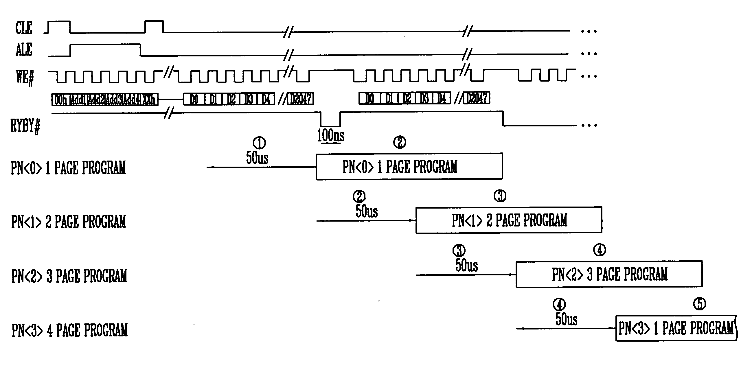
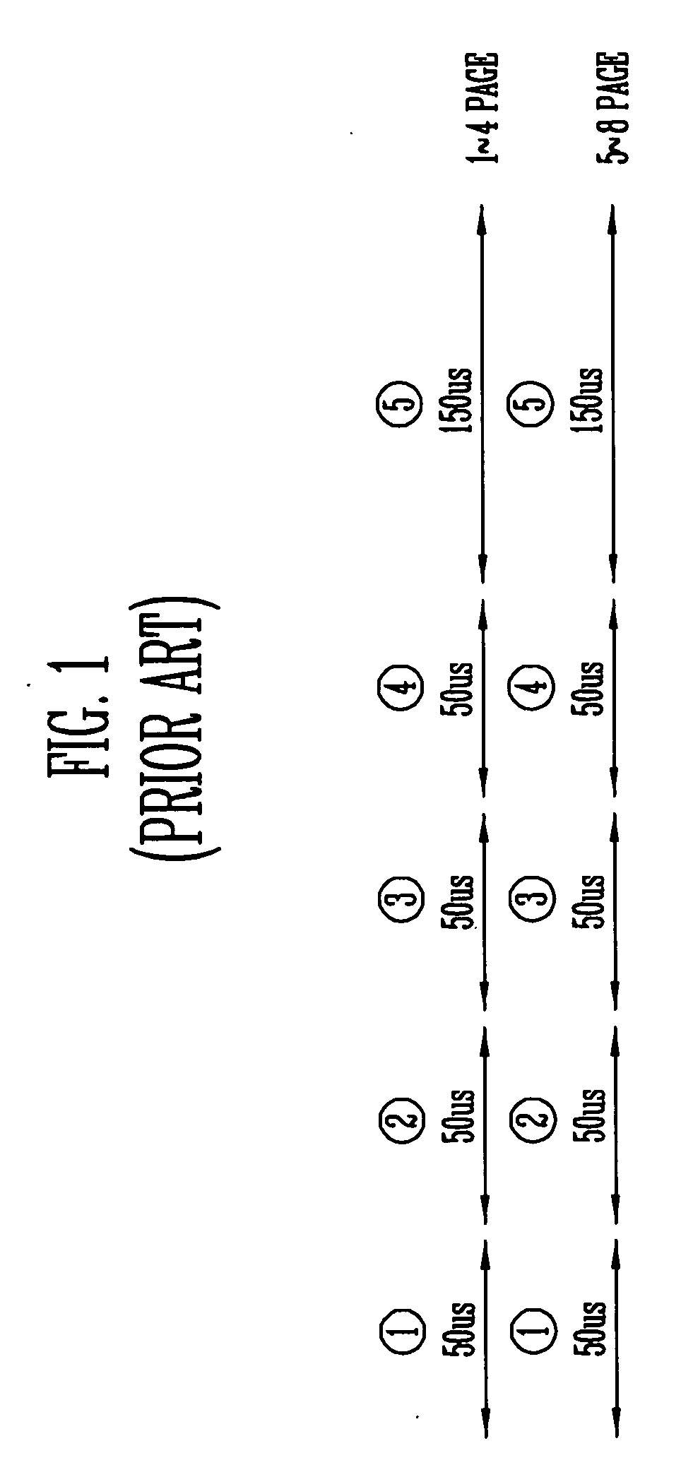
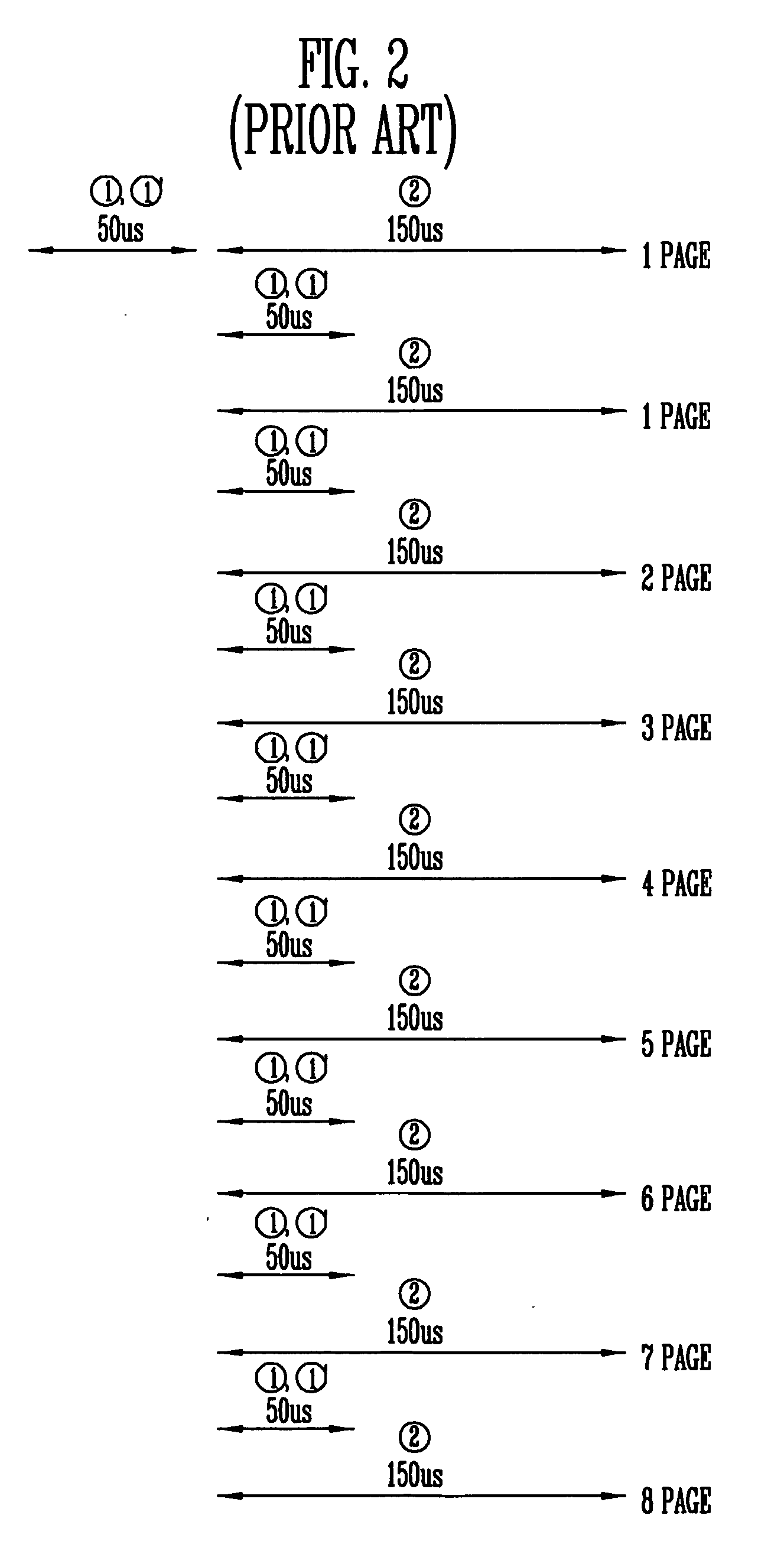
[0026] FIGS. 4 to 6 are views illustrating a multi-page program method of a NAND flash memory device having a multi-plane structure according to an embodiment of the present invention. FIG. 4 is a block diagram of the multi-page program method of the NAND flash memory device having the multi-plane structure. FIG. 5 is a timing diagram of a four-page program method of the NAND flash memory device having the 4-plane structure shown in FIG. 4. FIG. 6 is a timing diagram of an eight-page program method of the NAND flash memory device having the 4-plane structure shown in FIG. 4.

[0027] Referring to FIG. 4, the NAND flash memory device including the multi-plane structure includes four planes PN0> through PN3>. Although four planes are shown in FIG. 4, the number of planes may vary according to applications. Each of the planes PN0> through PN3> includes k...


PUM


Abstract

A method for performing a program operation of a non-volatile memory device includes loading first, second, third, and fourth data to first, second, third, and fourth page buffers, respectively, in sequence; programming the first data loaded onto the first page buffer into a first page while loading the second data to the second buffer; and programming the second data loaded onto the second page buffer into a second page while programming the first data into the first page.

Description

CROSS-REFERENCES TO RELATED APPLICATIONS [0001] The present application claims priority to Korean Patent Application No. 10-2005-86179, filed Sep. 15, 2005 and is incorporated by reference. BACKGROUND OF THE INVENTION [0002] The present invention relates to a program method of non-volatile memory devices, and more particularly, to a program method of NAND flash memory devices having a multi-plane structure. [0003] A NAND flash memory device has a low program speed, i.e., several hundreds of μs. Therefore, increasing program speed becomes an important parameter in enhancing the performance of a chip. To increase program speed, a variety of program operation methods such as “cache program” and “multi-page program” have been proposed. [0004]FIG. 1 illustrates an existing NAND flash memory device with a multi-plane structure using the multi-page program method. [0005] Referring to FIG. 1, the multi-page program method includes sequentially loading data onto a page buffer (not shown) on ...

Claims


Application Information

Patent Timeline
Patent Type & Authority Applications(United States)
IPC IPC(8): G06F13/28G06F12/00
CPCG06F12/0882G06F2212/2022G11C2216/14G11C16/10G11C16/32G11C16/0483G11C16/06
Inventor CHANG, SEUNG HOYANG, JOONG SEOB
Owner SK HYNIX INC
Learn More