Simulating circuit for magnetic tunnel junction device

a magnetic tunnel junction and simulation circuit technology, applied in the field of simulation circuits, can solve the problems of significant wires, reduce the capacity of current sources to output current, and no circuit model has been proposed for accurately simulating the write/read action of mtj devices, etc., and achieve the effect of reducing the ratio of current to output curren

Inactive Publication Date: 2007-03-22
IND TECH RES INST
View PDF8 Cites 7 Cited by
  • Summary
  • Abstract
  • Description
  • Claims
  • Application Information

AI Technical Summary

Benefits of technology

[0013] The circuit model for the MTJ device disclosed in the embodiments of the present invention can be applied for the circuit designing to simulate the write and read actions of the MTJ device. The model can describe the write action of the asteroid curve in the overall operation region of the MTJ device. After writing, the resistance of the MTJ device is automatically switched and memorized according to the write state (parallel or anti-parallel), and the effect of the Bias dependent MR Ratio (MR %) i.e., the MR ratio reduces as the read bias increases, can be simulated.

Problems solved by technology

However, from the already disclosed prior art so far, no circuit model has been proposed for accurately simulating the write / read actions of the MTJ device.
In addition, the write of the MTJ device all depends on the magnetic field generated by the current, thus another issue to be considered is that when designing the circuit of the current source, the wire resistances of the write word line and bit line assigned to each MTJ device should be accounted.
Particularly, when the memory array is enlarged, the load of the wires is significant, which may reduce the capacity of the current source to output current.

Method used


Image

  • Simulating circuit for magnetic tunnel junction device
  • Simulating circuit for magnetic tunnel junction device
  • Simulating circuit for magnetic tunnel junction device

Examples


Embodiment Construction

[0029] Reference will now be made in greater detail to a preferred embodiment of the invention, an example of which is illustrated in the accompanying drawings. Wherever possible, the same reference numerals are used throughout the drawings and the description to refer to the same or like parts. Reference in the specification to “one embodiment” or “an embodiment” means that a particular feature, structure, or characteristic described in connection with the embodiment is included in at least one embodiment of the invention. The appearances of the phrase “in one embodiment” in various places in the specification are not necessarily all referring to the same embodiment.

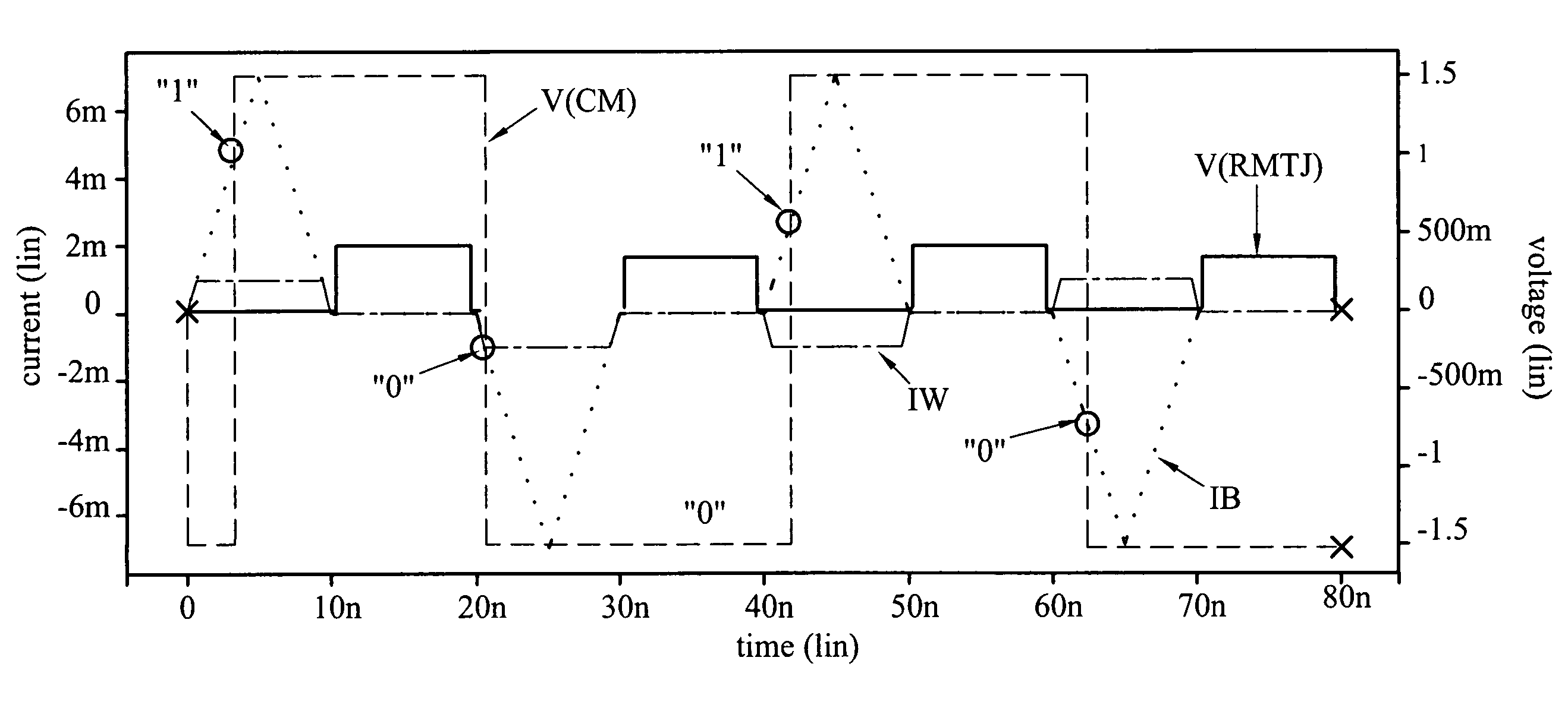
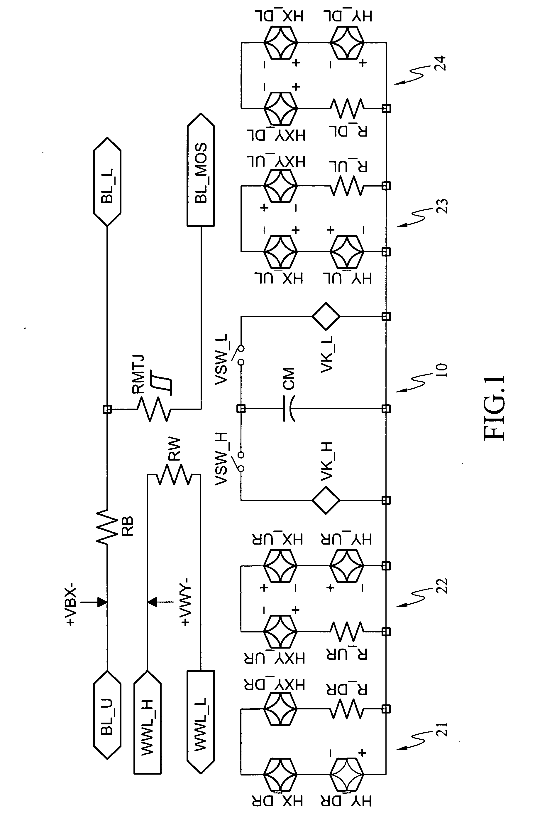
[0030] Referring to FIG. 1, which is a simulating circuit for the Magnetic Tunnel Junction Device, shows the equivalent circuits for writing in the four operation regions of the MTJ device.

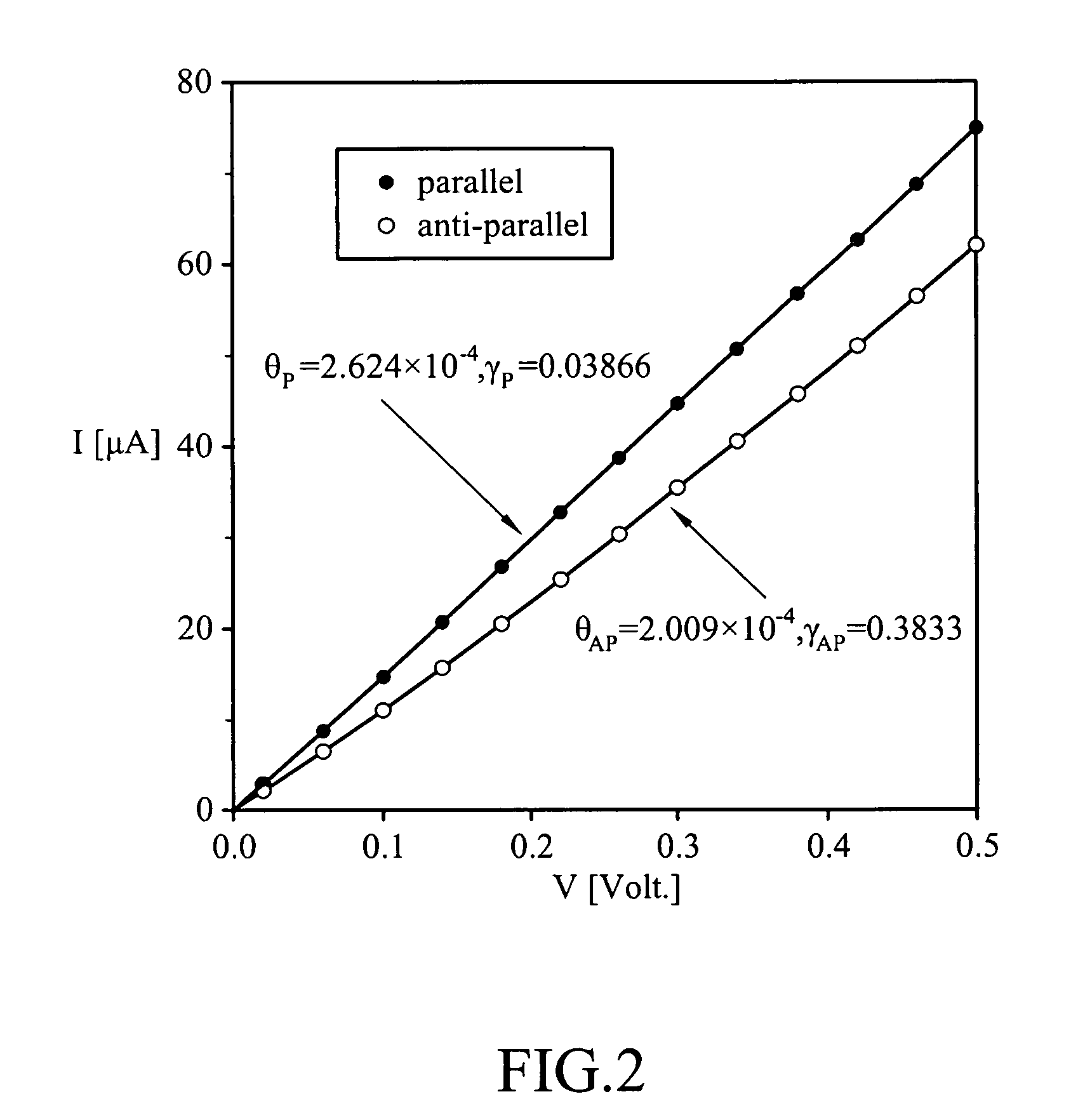
[0031] As for the magnetic memory, data (0 or 1) is recorded by the magnetization (parallel or anti-parallel) of the free layer an...


PUM


Abstract

A simulating circuit for simulating the operation of a magnetic tunnel junction (MTJ) device having at least a free layer and a fixed layer is provided. The simulating circuit includes a closed switch loop for simulating the magnetization of the free layer and the fixed layer, thus for simulating the data recording, wherein the magnetization includes parallel state or anti-parallel state; a first write loop for simulating the first quadrant of the operation region of the MTJ device; a second write loop, a third write loop, and a fourth write loop for simulating the second quadrant, the third quadrant, and the fourth quadrant of the operation regions, respectively; a first resistor for simulating the wire resistance of the bit lines; a second resistor for simulating the wire resistance of the write word lines; and a third resistor for simulating the resistance of the magnetic MTJ device.

Description

CROSS-REFERENCE TO RELATED APPLICATIONS [0001] This non-provisional application claims priority under 35 U.S.C. § 119(a) on Patent Application No(s). 94132731 filed in Taiwan, R.O.C. on Sep. 21, 2005 the entire contents of which are hereby incorporated by reference.BACKGROUND OF THE INVENTION [0002] 1. Field of the Invention [0003] The present invention relates to a simulating circuit, and more particularly to a circuit model for simulating the write and read actions of the magnetic tunnel junction (MTJ) device. [0004] 2. Related Art [0005] Magnetic Random Access Memory (MRAM) belongs to the non-volatile memory, which stores and records information by utilizing the resistance property, with the advantages of non-volatile, high intensity, high read and write speed, anti-radiation, etc. When writing data, the common method employs two current lines: bit line and write word line, wherein a memory unit selected by the intersection of the induction magnetic fields of the bit line and the...

Claims


Application Information

Patent Timeline
Patent Type & Authority Applications(United States)
IPC IPC(8): G11C11/14
CPCG06F17/5036G11C11/16G11C29/12005G11C2029/0403G11C29/50008G11C29/56004G11C29/56008G11C29/50G06F30/367
Inventor CHEN, YUNG-HSIANG
Owner IND TECH RES INST
Why Eureka
Try Eureka