Storage device and host apparatus

a storage device and host device technology, applied in the direction of memory adressing/allocation/relocation, instruments, input/output to record carriers, etc., can solve the problems of inability to predict the memory performance using a simple calculation, not the real rate, and the complexity of control

Active Publication Date: 2007-03-22
KIOXIA CORP
View PDF10 Cites 45 Cited by
  • Summary
  • Abstract
  • Description
  • Claims
  • Application Information

AI Technical Summary

Benefits of technology

[0011] According to a first aspect of the present invention, there is provided a storage device comprising: a semiconductor memory storing data; a controller instructing to write data to the semiconductor memory in accordance with a request the controller re

Problems solved by technology

However, it is often now the case that the storage device has a built-in controller; for this reason, the control has become complicated.
As a result, it is impossible to predict the memory performance using

Method used


Image

  • Storage device and host apparatus
  • Storage device and host apparatus
  • Storage device and host apparatus

Examples


first embodiment

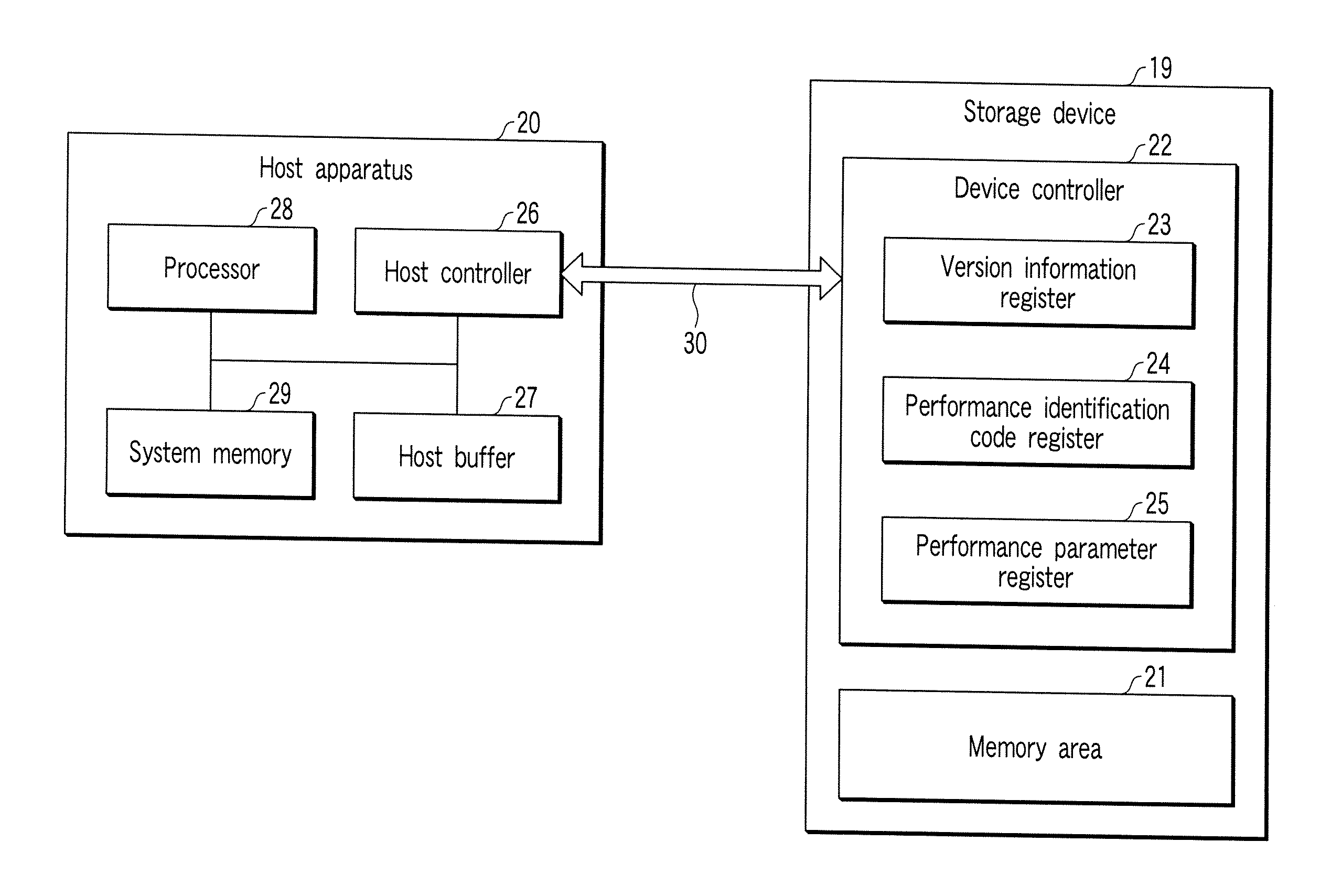
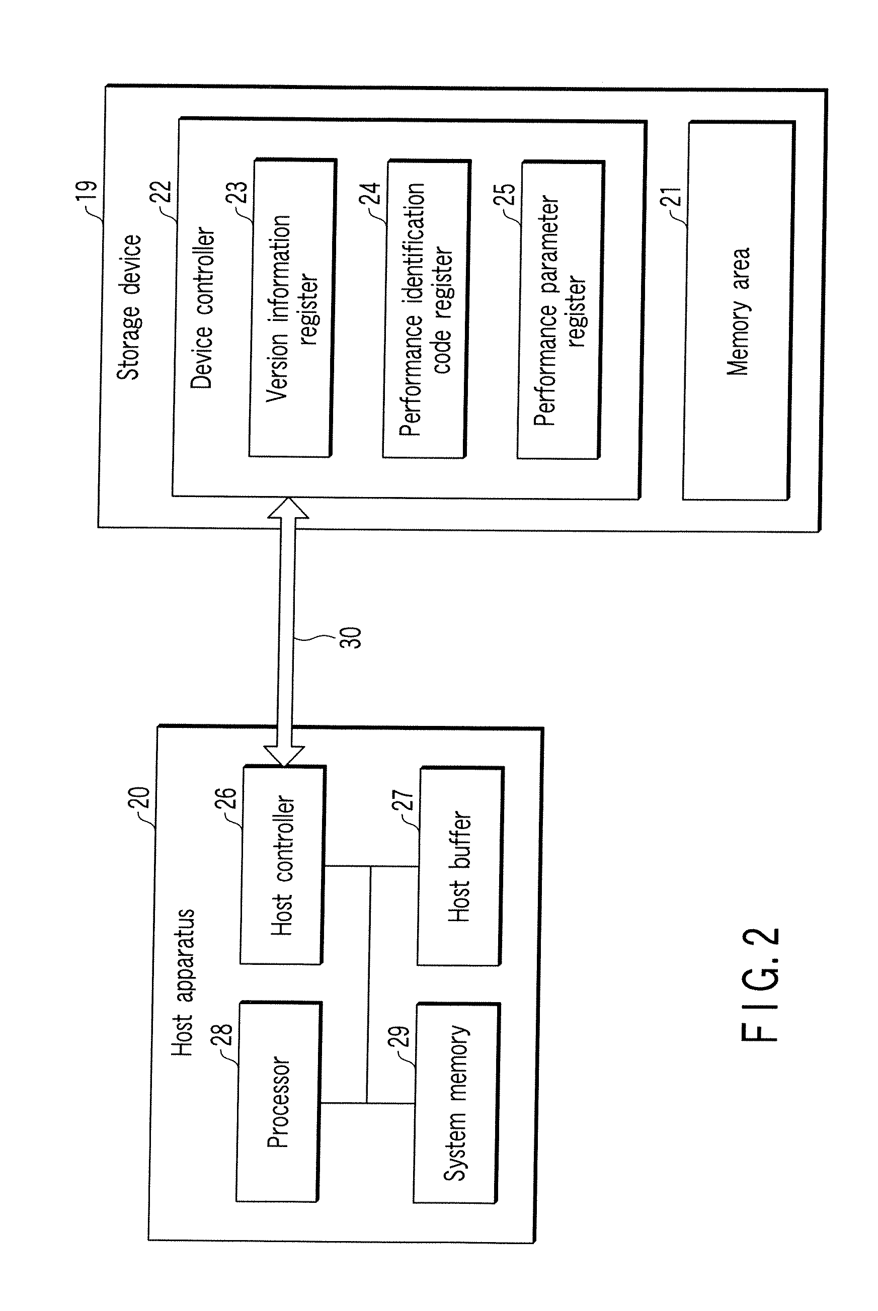
[0036] The first embodiment relates to a storage device having a built-in non-volatile semiconductor storage device, and to a host apparatus using the storage device.

[0037] [1] Configuration of Storage Device and Host Apparatus

[0038] In the following description, a NAND flash™ memory is used as a non-volatile semiconductor storage device built in a storage device used for the host apparatus according to the first embodiment of the present invention.

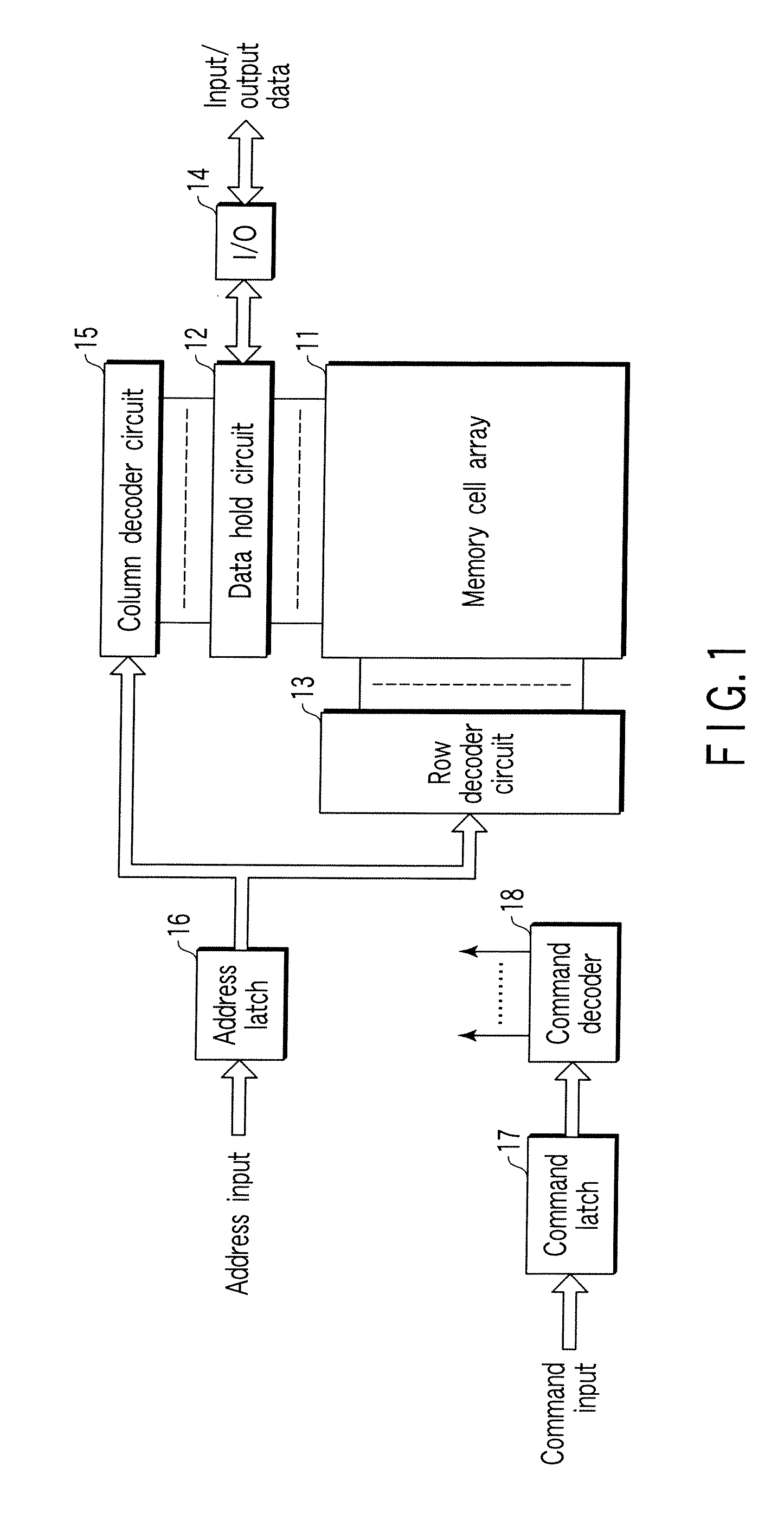
[0039]FIG. 1 is a block diagram showing the configuration of a semiconductor storage device (semiconductor memory) in the case of realizing the semiconductor storage device according to the first embodiment using a NAND flash™ memory.

[0040] In FIG. 1, a reference numeral 11 denotes a memory cell array. The memory cell array 11 is provided with several word lines, select gate lines and bit lines (not shown). The several word lines and bit lines are connected to several memory cells (not shown). The several memory cells are divided into...

second embodiment

[0248] An SD™ memory card to which the first embodiment is applicable will be explained below.

[0249]FIG. 17 is a schematic view showing the configuration of an SD™ memory card according to a second embodiment of the present invention. An SD™ memory card (hereinafter, referred simply to as memory card) 41 exchanges information with the host apparatus 20 via a bus interface 45. The memory card 41 includes NAND flash™ memory (hereinafter, referred simply to as flash memory) chip 42, card controller 43 controlling the flash memory chip 42, and several signal pins (first to ninth pins) 44. A reference numeral 45 denotes a bus interface.

[0250] The card controller 43 is equivalent to the device controller 22 of the first embodiment (see FIG. 2). The flash memory 42 is equivalent to the memory area 21 of FIG. 2.

[0251] The signal pins 44 are electrically connected to the card controller 43. Signal allocation to signal pins 44, that is, first to ninth pins are as shown in FIG. 18.

[0252] D...


PUM


Abstract

A storage device includes a semiconductor memory storing data. A controller instructs to write data to the semiconductor memory in accordance with a request the controller receives. A register holds performance class information showing one performance class required to allow the storage device to demonstrate best performance which the storage device supports, of performance classes specified in accordance with performance.

Description

CROSS-REFERENCE TO RELATED APPLICATIONS [0001] This is a Continuation Application of PCT Application No. PCT / JP2005 / 013104, filed Jul. 8, 2005, which was published under PCT Article 21(2) in English. [0002] This application is based upon and claims the benefit of priority from prior Japanese Patent Applications No. 2004-204028, filed Jul. 12, 2004; and No. 2004-342275, filed Nov. 26, 2004, the entire contents of both of which are incorporated herein by reference. BACKGROUND OF THE INVENTION [0003] 1. Field of the Invention The present invention relates to a storage device and a host apparatus (electronic apparatus) using a storage device. In particular, the present invention relates to a storage device such as a non-volatile semiconductor storage device and a memory card using it. In addition, the present invention relates to an electronic apparatus such as a recording apparatus; for example, a digital still camera and a digital video camera having the storage device built in. For e...

Claims


Application Information

Patent Timeline
IPC IPC(8): G06F12/00
CPCG06F3/061G06F3/0632G06F12/0246G06F13/385G11C16/20G06F3/0679G06F3/06G06F12/00G06F12/06G06F3/0613G06F3/0634G06F2206/1014
Inventor FUJIMOTO, AKIHISA
Owner KIOXIA CORP
Why Eureka
Try Eureka