Method for manufacturing an integrated semiconductor device

a semiconductor device and manufacturing method technology, applied in semiconductor devices, semiconductor/solid-state device details, electrical devices, etc., can solve the problems of obstructing communication, affecting the quality of integrated semiconductor devices, and unwanted signals on the second conductor interfere with wanted signals on the second conductor, etc., to achieve low capacitive coupling, low cost, and easy processing

Inactive Publication Date: 2007-03-29
INFINEON TECH AG
View PDF7 Cites 11 Cited by
  • Summary
  • Abstract
  • Description
  • Claims
  • Application Information

AI Technical Summary

Benefits of technology

[0012] Later on, the sacrifice structure is removed thereby generating a void, or cavity, in place of the sacrifice structure. The void is either filled with low k material or with air or any other gas. In the latter case it is advantageous to coat the walls of the void with an electrically insulating film preventing an electrical break down. Further, it is advantageous to seal the void from the environment of the device thereby preventing the intrusion of any material into the void.
[0014] The present invention provides an advantage that the sacrifice structure is easily processed and no constraints need to be considered or observed in the design of the processing of the integrated semiconductor device, but a low capacitive coupling between proximate conductors is provided. The present invention is particularly advantageous for integrated semiconductor memory devices with minimum distances between bit lines or between bit lines and via conductors vertically connecting a cell transistor, or selection transistor, with a storage capacitor. According to the present invention self-aligning techniques and minimum distances even far below the lithography resolution are combined with low capacitive coupling.

Problems solved by technology

Miniaturization of integrated semiconductor devices is a permanent issue with multifaceted challenges.
This unwanted signal on the second conductor interferes with wanted signals on the second conductor.
In the worst case the unwanted signal obstructs in communication, or exchange of data, via the second conductor.

Method used


Image

  • Method for manufacturing an integrated semiconductor device
  • Method for manufacturing an integrated semiconductor device
  • Method for manufacturing an integrated semiconductor device

Examples


Embodiment Construction

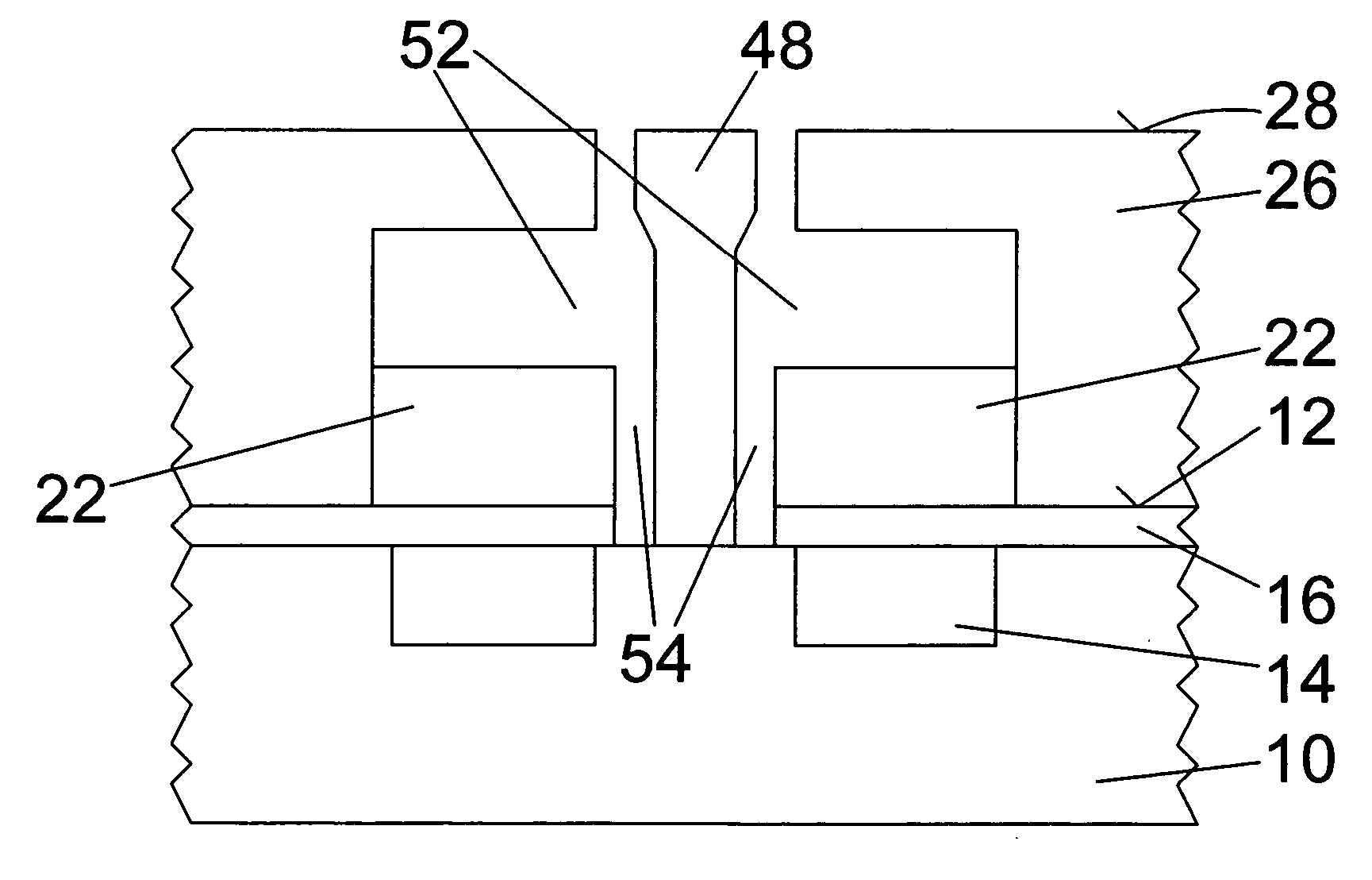
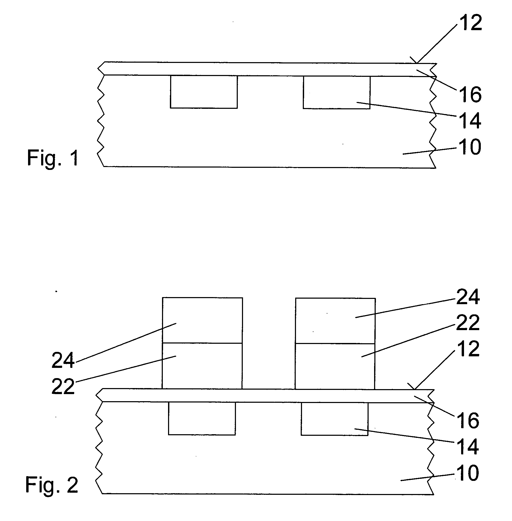
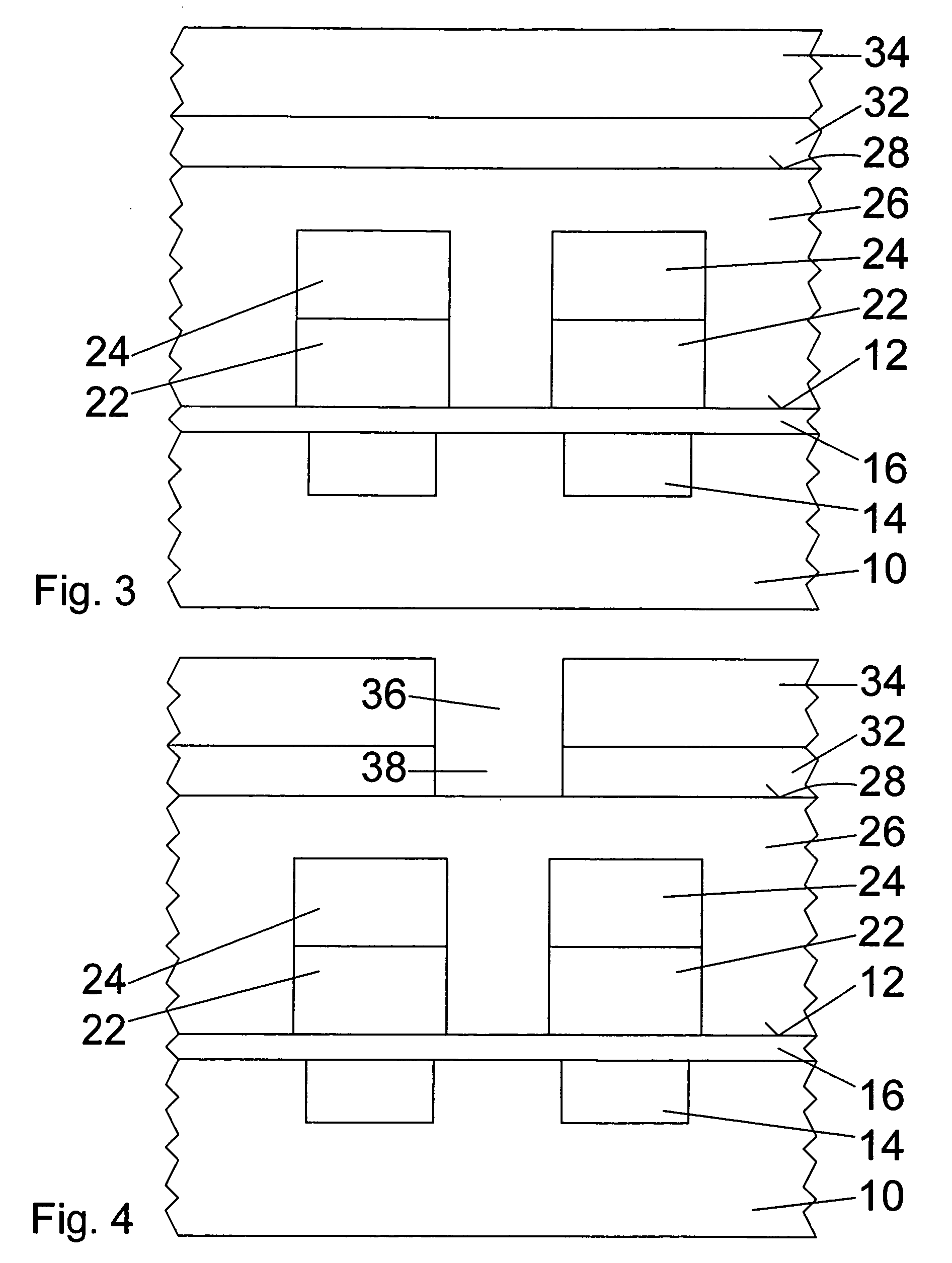
[0022] The FIGS. 1 to 26 display schematic views of cross sections of integrated semiconductor devices according to embodiments of the present invention. The cross section is always vertical, or perpendicular to a main surface of the substrate of the integrated semiconductor device. The Figures show different stages of the manufacturing process of the integrated semiconductor device.

[0023] The integrated semiconductor device is exemplified by an integrated semiconductor memory device. However, the present invention can be applied to any other kind of integrated semiconductor device as well. As already mentioned above, the present invention is particularly advantageous for highly miniaturized devices with a minimum distance between proximate conductors. In the example of the memory device, these proximate conductors with minimum distance are represented by a laterally elongated bit line and a vertically elongated via conductor vertically connecting a cell transistor, or selection tr...


PUM


Abstract

In a method for manufacturing an integrated semiconductor device with low capacitive coupling between a conductive member and a via, a semiconductor substrate with a surface is provided. The conductive member is formed on the surface of the substrate wherein the conductive member is provided for conducting a current in a direction parallel to the surface of the substrate. A sacrifice structure is produced. A via is formed for conducting a current in a direction vertical to the surface of the substrate. The sacrifice structure at least partially defines the shape and position of the via and separates the conductive member and the via. The sacrifice structure is removed thereby generating a void in place of the sacrifice structure.

Description

TECHNICAL FIELD OF THE INVENTION [0001] The present invention relates to a method for manufacturing an integrated semiconductor device and to an integrated semiconductor device with low capacitive coupling between two proximate conductors. BACKGROUND OF THE INVENTION [0002] Miniaturization of integrated semiconductor devices is a permanent issue with multifaceted challenges. The linear dimensions of the microscopic structures of an integrated semiconductor device have a strong influence on the capacitive coupling between conductors of the device. The smaller the distance between two proximate conductors is, the higher is their mutual electrostatic capacitance and the stronger is their capacitive coupling. Due to capacitive coupling, the wanted signal on a first conductor generates an unwanted signal on a second conductor proximate to the first conductor. This unwanted signal on the second conductor interferes with wanted signals on the second conductor. Being a kind of noise the unw...

Claims


Application Information

Patent Timeline
Patent Type & Authority Applications(United States)
IPC IPC(8): H01L29/00H01L21/4763
CPCH01L21/7682H01L21/76834H01L21/76897H01L2221/1057H01L23/53295H01L27/10855H01L27/10885H01L23/5222H01L2924/0002H01L2221/1063H10B12/0335H10B12/482H01L2924/00
Inventor TEGEN, STEFANMUMMLER, KLAUSBAARS, PETER
Owner INFINEON TECH AG
Why Eureka
Try Eureka