Semiconductor device

a technology of semiconductor devices and semiconductors, applied in semiconductor devices, semiconductor/solid-state device details, instruments, etc., can solve the problems of weak dynamic stress, short communication distance, easy destruction, etc., and achieve the effect of improving the mechanical strength of the joining against bending stress applied from various directions, improving the strength, and improving the mechanical strength at the joining poin

Inactive Publication Date: 2007-03-29
SEMICON ENERGY LAB CO LTD
View PDF21 Cites 6 Cited by
  • Summary
  • Abstract
  • Description
  • Claims
  • Application Information

AI Technical Summary

Benefits of technology

[0012] The present invention provides a semiconductor device of which mass production is possible and the structure is different from that of a conventional small-size element. In addition, it is an object of the invention to provide a structure of a semiconductor device of which the strength can be improved, destruction of an element in manufacturing can be suppressed, and the reliability and yield are high, and a manufacturing method of the semiconductor device.
[0025] By using the structure of the present invention, mechanical strength at a joining point can be improved. Further, by providing three or more terminals, a plane surface can be formed two-dimensionally, thereby the terminal does not become a fulcrum of bending stress, unlike conventionally, even when bending stress is applied to an element (e.g., a transistor included in a semiconductor device), so that the element can be designed without damaging reliability. For example, in the case of three terminals, a triangle plane surface with vertexes of the three terminals can be formed, and thus bending stress applied to the element can be dispersed within the surface.
[0026] In addition, by increasing the number of joining terminals according to the structure of the present invention, mechanical strength of joining against bending stress applied from various directions can be improved, and redundancy can also be provided. In addition, in the case of using a terminal which does not affect electrically (a pseudo terminal), the pseudo terminal can be designed at an arbitrary position within the element even when there is area limitation of a wiring or when wirings are provided so as to be concentrated within the element surface, which can contribute to dispersion of stress of an electrical joining terminal. Furthermore, by providing the pseudo terminal so as to be symmetric to the electrical joining terminal, various bending stress can be dispersed, thereby strength can be improved. Further, in a manufacturing step, a load is dispersed evenly to the plurality of terminals even in a pressure bonding method that is a joining method of the element and the antenna, thereby destruction of the element can be suppressed so that the yield can be improved.

Problems solved by technology

However, a flexible product manufactured by joining the element and the antenna to each other has such a problem that it is weak against dynamic stress, e.g., bending or twisting, and is easy to destroy.
Therefore, a semiconductor device with a built-in antenna has such a problem that the size of the antenna is restricted, and thus communication distance thereof becomes short.
In addition, there is such a problem that since the element area is restricted, the size and / or kind of memory capacity or the like is limited.
Furthermore, in the case where the element area is small, since a wide area for forming a terminal cannot be obtained, a device in which a terminal is provided over the element with an insulating layer interposed therebetween, or the like is required in addition to the above-described limitation.
In addition, in the case where the number of terminals is small, a load in pressure-bonding between an antenna material and the terminal is concentrated at the terminal portion, which destroys the element itself, or the load applied to each terminal is varied, thereby causing decrease in the yield.

Method used


Image

  • Semiconductor device
  • Semiconductor device
  • Semiconductor device

Examples


embodiment mode 1

(Embodiment Mode 1)

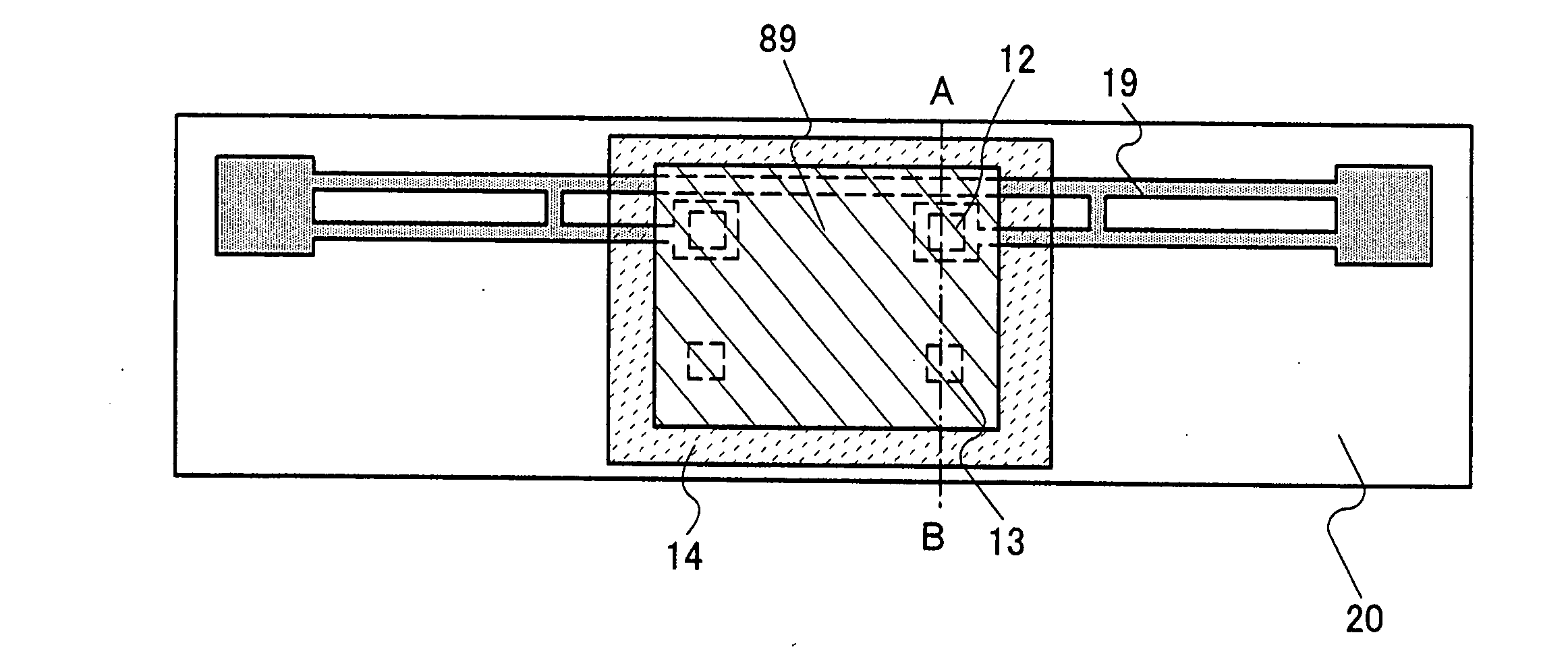
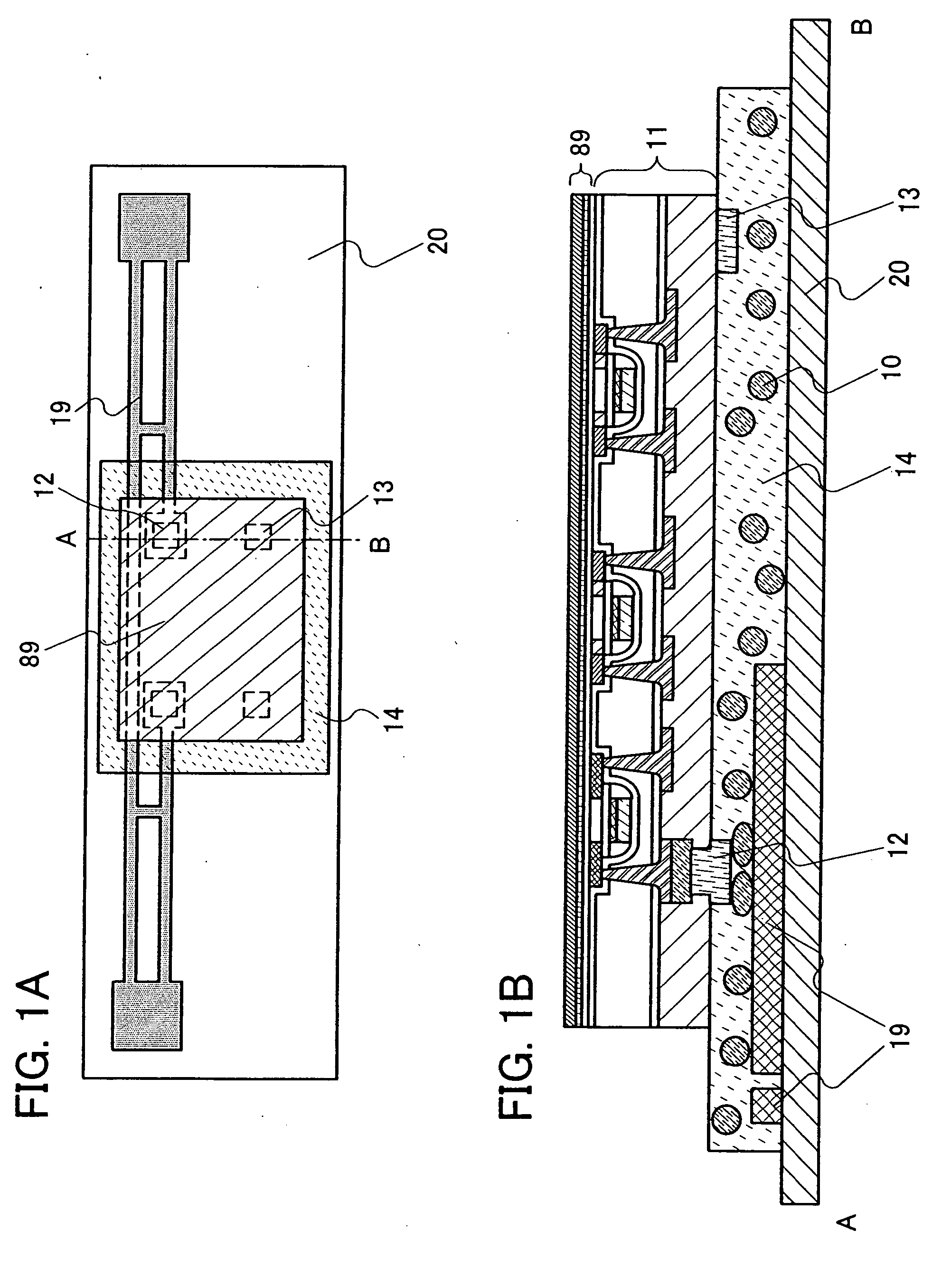
[0051] A structure of a semiconductor device in this embodiment mode is described with reference to FIGS. 1A and 1B, and 2A and 2B. FIG. 1B is a cross-sectional diagram along a line A-B of a top diagram of FIG. 1A. FIG. 2B is a cross-sectional diagram along a line A-B of a top diagram of FIG. 2A.

[0052] A substrate 89 and a substrate 20 are provided such that one surface of the substrate 89 and one surface of the substrate 20 face each other. On the one surface of the substrate 89, a layer 11 including an integrated circuit is formed (see FIG. 1B and FIG. 2B). Over the layer 11 including the integrated circuit, a terminal 12 which is electrically connected to a wiring included in the layer 11 including the integrated circuit is provided. Note that the layer 11 including the integrated circuit includes a plurality of transistors. The terminal 12 is electrically connected to a conductive layer 19 which functions as an antenna formed on the one surface of the substra...

embodiment mode 2

(Embodiment Mode 2)

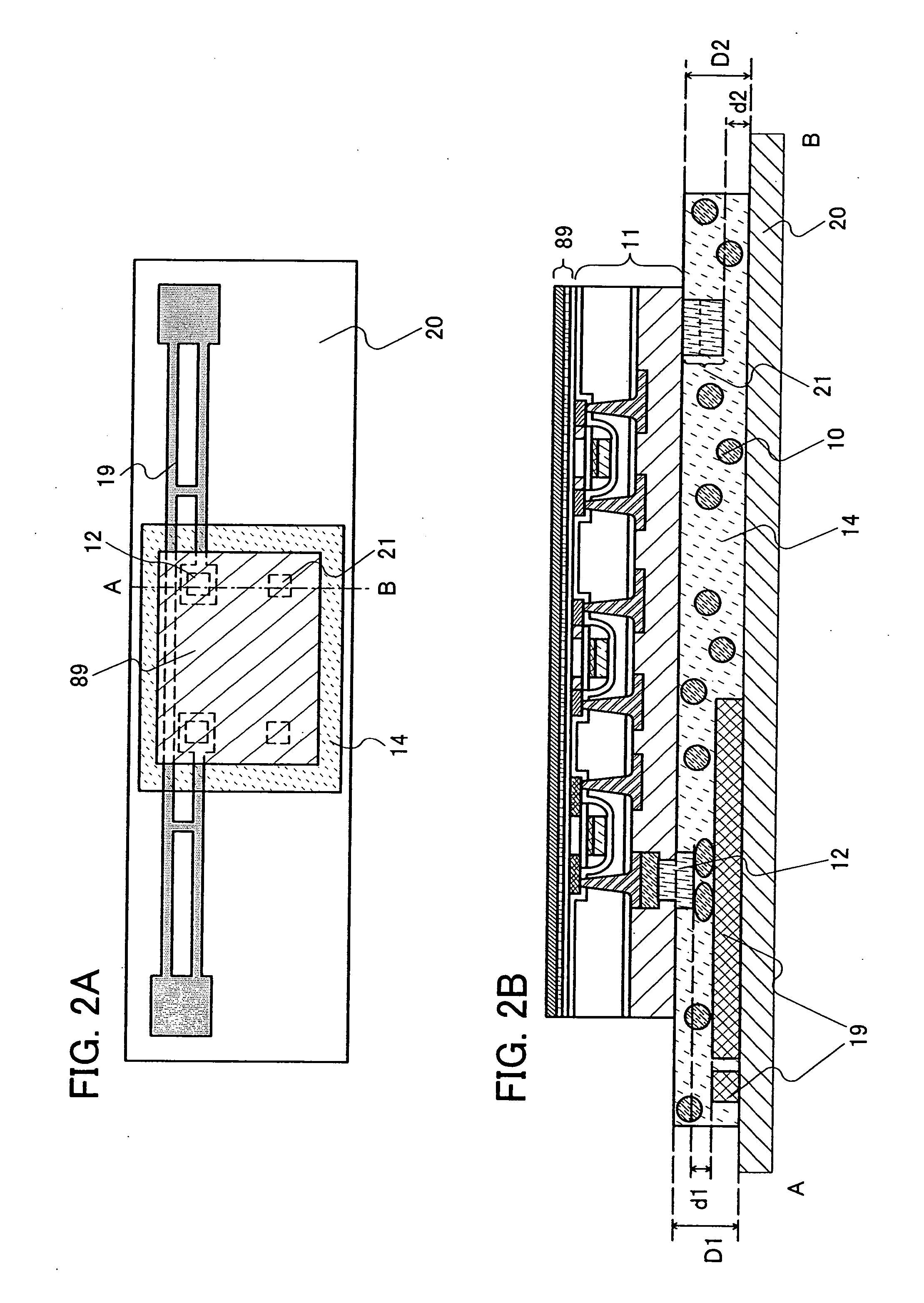
[0057] This embodiment mode describes a structure of a semiconductor device of which the shape is different from the semiconductor device described in Embodiment Mode 1, with reference to FIGS. 3A and 3B. This embodiment mode is different from the structure described in Embodiment Mode 1 in that a layer formed of a conductive material is provided in addition to a conductive layer which functions as an antenna, for a substrate provided with the conductive layer which functions as the antenna on one surface thereof. Note that description of the same points as Embodiment Mode 1 is omitted.

[0058] As shown in FIGS. 3A and 3B, an element of the invention includes the pseudo terminal 13 over the layer 11 including the integrated circuit. Note that the number and position of the pseudo terminals of the invention are not limited to the structure shown in the drawing. That is, the position and number of the pseudo terminals can be freely changed as long as the pseudo termi...

embodiment mode 3

(Embodiment Mode 3)

[0063] An embodiment mode of the invention is described with reference to FIGS. 4A and 4B. This embodiment mode describes a structure of a semiconductor device of which the shape is different from those of Embodiment Mode 1 and Embodiment Mode 2. This embodiment mode is different from Embodiment Mode 1 and Embodiment Mode 2 in the shape of the conductive layer which functions as the antenna and in that a plurality of terminals (hereinafter abbreviated as auxiliary terminals) which are electrically connected to the conductive layer which functions as the antenna, in addition to the terminal which is electrically connected to the conductive layer which functions as the antenna are provided. Note that description of the same points as Embodiment Mode 1 is omitted.

[0064] As shown in FIGS. 4A and 4B, over the layer 11 including the integrated circuit, an auxiliary terminal 24 which is electrically connected to both of the wiring included in the layer 11 including the ...


PUM


Abstract

The invention includes a layer having an integrated circuit, a first terminal which is formed over the layer having the integrated circuit and is electrically connected to the layer having the integrated circuit, a conductive layer which functions as an antenna, which is formed over the first terminal and is electrically connected to the first terminal, and a second terminal which is formed over the layer having the integrated circuit and is not electrically connected to the layer having the integrated circuit, the conductive layer which functions as the antenna, and the first terminal.

Description

BACKGROUND OF THE INVENTION [0001] 1. Field of the Invention [0002] The present invention relates to a semiconductor device having a memory, a microprocessor (central processing unit, MPU), or the like and mounted with a thin film integrated circuit, which is thin and flexible like paper. In addition, the present invention relates to a non-contact type semiconductor device having the thin film integrated circuit and an antenna, which is used mainly for a card, a tag, a label, or the like for identifying human beings, animals and plants, commercial products, banknotes, or the like. [0003] 2. Description of the Related Art [0004] In recent years, a semiconductor device capable of transmitting and receiving data has been actively developed, and such a semiconductor device is called an IC chip, an RF tag, a wireless tag, an electronic tag, a wireless processor, a wireless memory, or the like. Although the semiconductor devices which have been put into the practical use are mainly use si...

Claims


Application Information

Patent Timeline
Patent Type & Authority Applications(United States)
IPC IPC(8): H01L23/48
CPCG06K19/07749G06K19/0775H01L23/49855H01L23/5389H01L2223/6677H01L2924/04941H01L2924/01004H01L2924/01046H01L2924/01077H01L2924/01078H01L2924/01079H01L2224/16H01L2924/12044H01L2924/00
Inventor KUSUMOTO, NAOTOTAKAHASHI, HIDEKAZUKOBAYASHI, YUKA
Owner SEMICON ENERGY LAB CO LTD
Why Eureka
Try Eureka