Display device

a technology of display device and display screen, which is applied in the direction of discharge tube/lamp details, discharge tube luminescent screen, discharge tube/lamp details, etc., can solve the problems of reducing the life of the element, power consumption, contrast or deterioration of image quality, etc., and achieves good visibility and quiet ambient light.

Inactive Publication Date: 2007-03-29
CANON KK
View PDF10 Cites 24 Cited by
  • Summary
  • Abstract
  • Description
  • Claims
  • Application Information

AI Technical Summary

Benefits of technology

[0012] The present invention has been accomplished in view of the above-mentioned problems, and an object of the present invention is to provide a display device which quenches ambient light by using only an optical interference effect without additionally using an optical filter such as a color filter, and can provide good visibility out of doors in the daylight.

Problems solved by technology

Accordingly, for example, when a display device is used out of doors, the reflection of ambient light or the reflection of outside scenery occurs, thereby leading to a reduction in contrast or the deterioration of image quality.
Accordingly, when an attempt to obtain a desired luminance is to be made, the organic EL element needs to generate luminance which is twice or more the desired luminance, with the result that the power consumption increases.
In addition, a high load is applied to the element, so that there is posed a problem such as a reduction in the lifetime of the element.
Further, the method disclosed in Japanese Patent Application Laid-Open No. 2002-373776 requires the step of forming the light-absorbing filter on a pixel, thereby causing a problem that a production process for a display device becomes complicated.
As shown in FIG. 20, a conventional ambient light quenching method according to an optical interference system has posed a problem that because in a light-emitting pixel portion of, for example, a blue or red emission color, the reflection of ambient light in a green color region cannot be sufficiently reduced, whereby the contrast of a display device is reduced.
Accordingly, when the method is to be applied to a display device constituted by a plurality of organic EL elements of different emission colors, another optical means such as a color filter needs to be used in combination, thereby posing a problem that the constitution of the display device becomes complicated and the production cost of the device is high.

Method used


Image

  • Display device
  • Display device
  • Display device

Examples


example 1

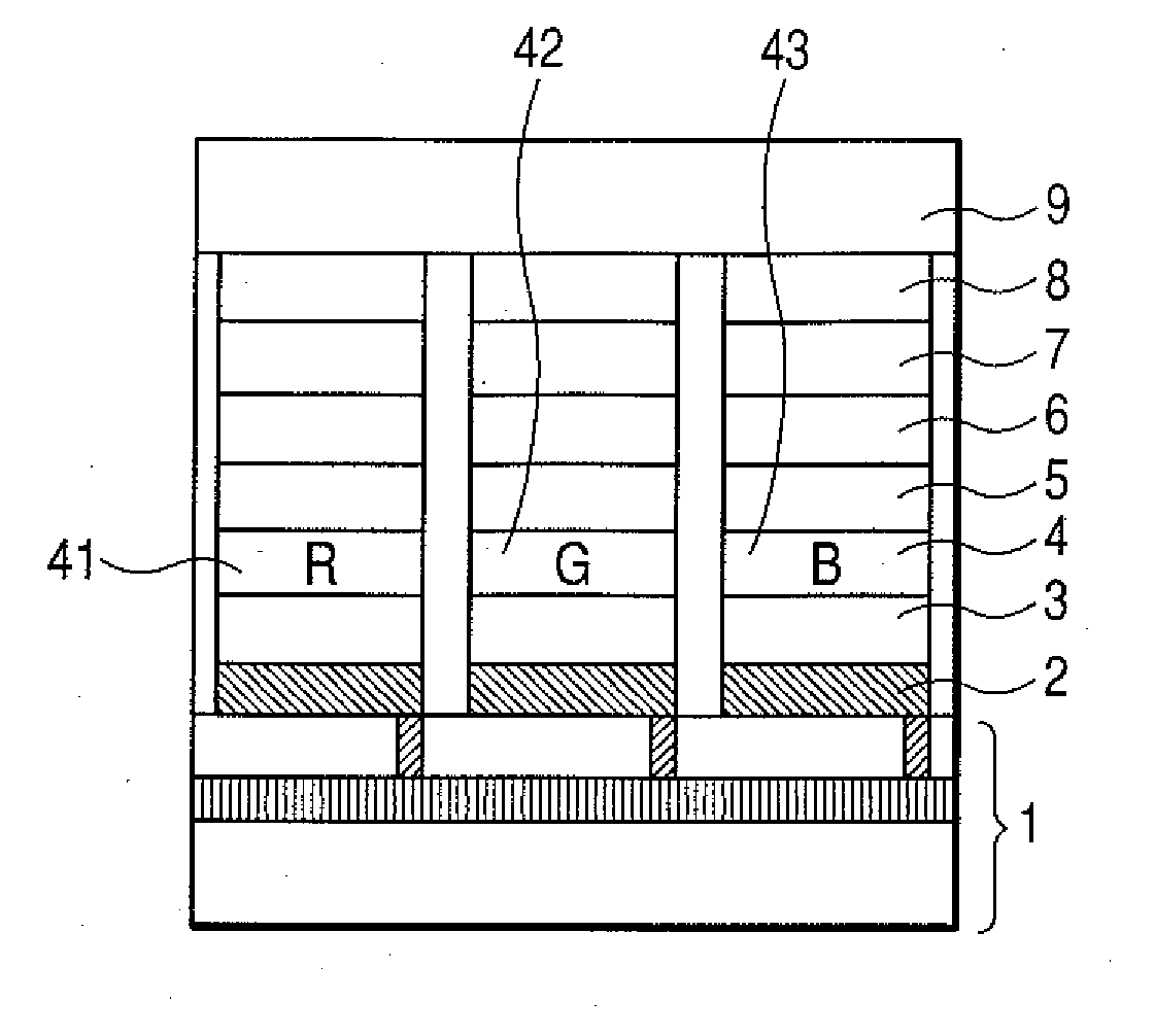
[0101] A display device of three colors R, G, and B having a structure shown in FIG. 12 was produced by the following method.

[0102] On a glass sheet as a support member 11 was formed a TFT drive circuit 12 composed of low-temperature polysilicon, and a flattening layer 13 composed of an acrylic resin was formed thereon to prepare a substrate 1.

[0103] A reflective layer 21 was formed thereon by sputtering an aluminum alloy (AlNiPd) in a thickness of about 100 nm, followed by patterning. Further, a transparent conductive film 22 was formed thereon by sputtering IZO in a thickness of 20 nm, followed by patterning, whereby the reflective electrode 20 was formed. Further, an element separation film 23 was formed of an acrylic resin, whereby the substrate having the reflective electrode 20 formed thereon was prepared. The thus prepared substrate was subjected to ultrasonic cleaning with isopropyl alcohol (IPA), and was then subjected to boil washing followed by drying. Further, the drie...

example 2

[0116] A display device was produced by following the same procedure as in Example 1 with the exception that the thickness of the organic compound layer and the thickness of the reflectance-adjusting layer were optimized for each emission color individually as shown in Table 3.

[0117]FIG. 14 shows the ambient light reflection characteristics of the display device thus obtained. In this example, the ambient light reflection characteristics vary for each light-emitting pixel because the film thickness is set for each emission color individually. In addition, Table 5 shows the results of the evaluation made in a manner similar to that of Example 1. Incidentally, the contrast value in this example is the average of the contrast values of the respective R, G, and B light-emitting pixels.

TABLE 3RedGreenBlueReflectance-adjusting layerSiO230 nm30 nm30 nmWC25 nm25 nm30 nmSiO295 nm180 nm 180 nm Cathode10 nm10 nm10 nmElectron injection layer30 nm10 nm10 nmElectron-transporting layer10 nm10 n...


PUM


Abstract

There is provided a display device which quenches ambient light by using only an optical interference effect without additionally using an optical filter such as a color filter, and can provide good visibility out of doors in the daylight. The display device includes a plurality of organic EL elements each having a light extraction electrode, a reflective electrode, and a plurality of organic compound layers disposed between the electrodes, wherein the plurality of organic EL elements include at least organic EL elements which emit a red light, a green light, and a blue light, respectively; a layer comprised of a material having anomalous dispersion is disposed at a location which is on a light extraction side with respect to the reflective electrode in each of the plurality of organic EL elements; and an ambient light reflectance of the display device shows a minimal in a region of 535 nm or more and 575 nm or less.

Description

BACKGROUND OF THE INVENTION [0001] 1. Field of the Invention [0002] The present invention relates to a display device employing light-emitting elements using an organic compound, and more particularly, to a display device using organic electroluminescence (EL) elements that emit light when an electric field is applied to a thin film comprised of an organic compound. [0003] 2. Description of the Related Art [0004] Organic EL elements (organic light-emitting elements or organic electroluminescence elements) have been actively researched and developed in recent years. When a display device utilizing any one of such organic EL elements is used in an outdoor environment, ambient light is incident on the organic EL element through a transparent electrode, is reflected on a metal electrode inside the element, is emitted from the transparent electrode, and returns to the outside of the element again. Accordingly, for example, when a display device is used out of doors, the reflection of amb...

Claims


Application Information

Patent Timeline
Patent Type & Authority Applications(United States)
IPC IPC(8): H01J1/62H01J63/04
CPCC09K11/06C09K2211/1011C09K2211/1014H05B33/14C09K2211/1088C09K2211/186H01L51/5281C09K2211/1037H10K50/86
Inventor HASEGAWA, TOSHINORIMATSUDA, HIROSHIOKUDA, MASAHIROYASHIMA, MASATAKAFUKUDA, KOICHIMIZUNO, NOBUTAKA
Owner CANON KK
Why Eureka
Try Eureka