Semiconductor radiation detectors and method for fabrication thereof

a radiation detector and semiconductor technology, applied in semiconductor/solid-state device manufacturing, electric devices, solid-state devices, etc., can solve the problems of inability to thin, additional undesirable diffusion of profiles, and crystal damage that needs to be eliminated

Inactive Publication Date: 2007-03-29
KEMMER JOSEF
View PDF3 Cites 29 Cited by
  • Summary
  • Abstract
  • Description
  • Claims
  • Application Information

AI Technical Summary

Problems solved by technology

A further drawback of implantation doping is that it causes crystal damage which needs to be eliminated by subsequent temperature treatment.
This, however, results in an additional undesirable diffusion of the profiles.
These layers thus have the drawback that they cannot be made thin as one would prefer and that their effective thickness depends on the applied operating voltage of the detector and on the thermal annealing parameters.
Indeed, a further change

Method used


Image

  • Semiconductor radiation detectors and method for fabrication thereof
  • Semiconductor radiation detectors and method for fabrication thereof
  • Semiconductor radiation detectors and method for fabrication thereof

Examples


Embodiment Construction

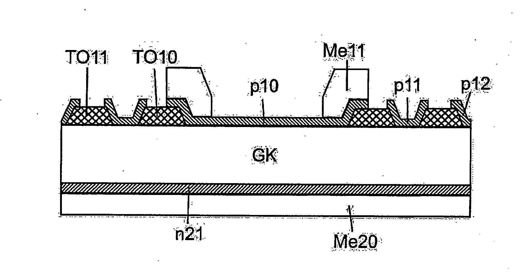
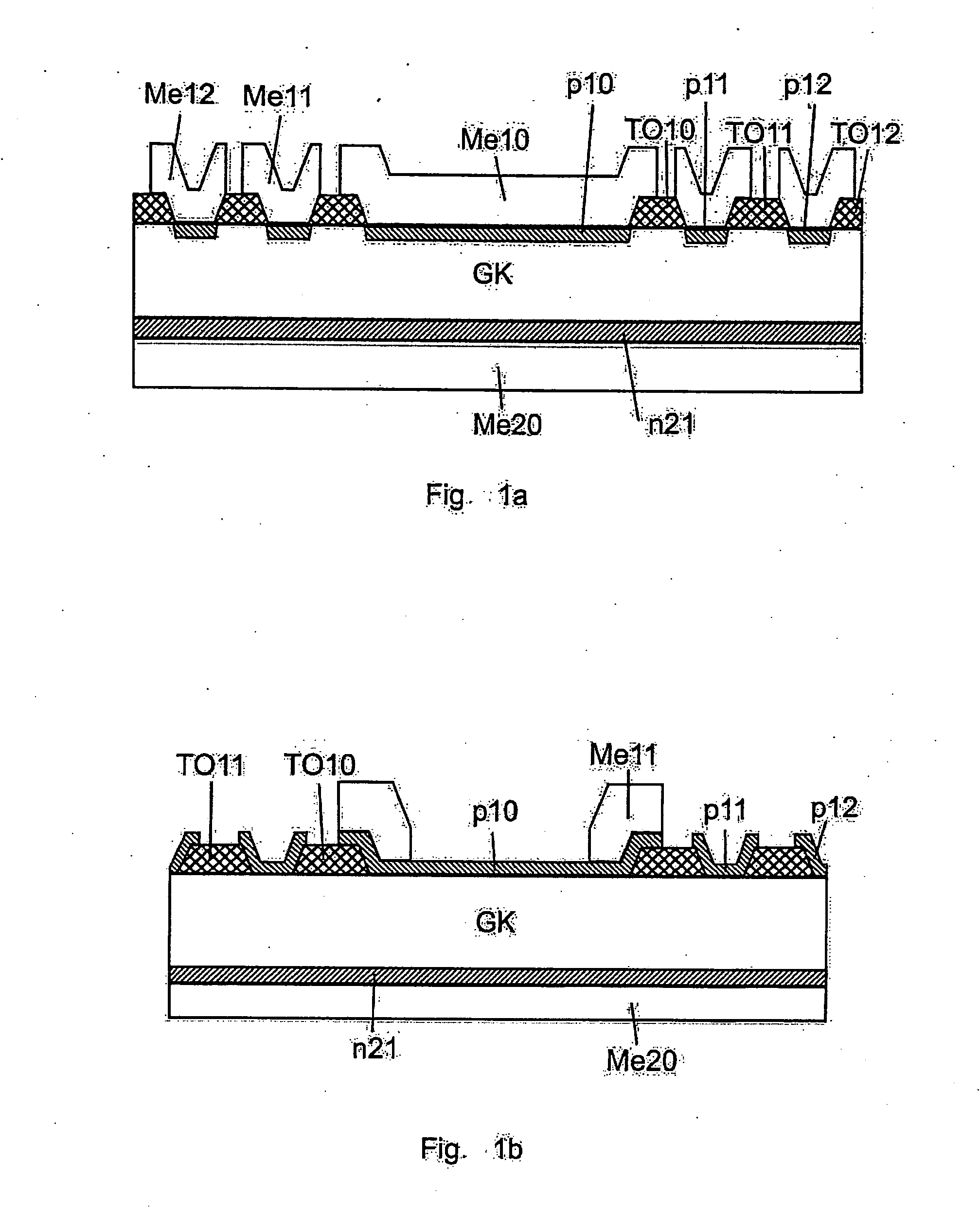
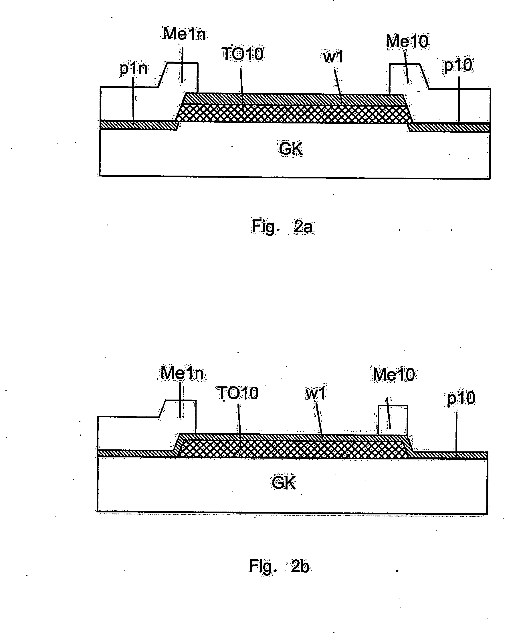
[0029] Like elements are identified by like reference numerals in the following figures to avoid repeat descriptions -of the elements already described in discussing the individual figures.

[0030] Before proceeding further with the detailed description of FIG. 1, however, a few items of the embodiments will be discussed.

[0031] In accordance with the embodiments of the invention it has now been discovered that by applying epitaxy instead of ion implantation for forming the further semiconductor layers of at least one of the second and the first conductivity type on the semiconductor body, all of the above-mentioend drawbacks can be avoided.

[0032] With the aid of a method according to an embodiment it is now possible to vary the layer thickness and dopant concentration within broad limits. There is no problem technically in generating with the aid of suitable epitaxy methods sharp doping profiles, indeed even so-called delta layers. Since doping concentrations up to 10E21 per cm are...


PUM


Abstract

The invention relates to a method for fabricating semiconductor radiation detectors comprising a bulk of a first conductivity type for detecting radiation with further semiconductor layers of a second and a first conductivity type patterned thereon, at least one of the further semiconductor layers being deposited by epitaxy. The invention relates further to integration of electronic components in radiation detectors in employing epitaxy, as well as to radiation detectors of a great variety in which epi layers are deposited as thin radiation entrance windows, as guard structures and as resistive layers.

Description

FIELD OF THE INVENTION [0001] The present invention relates generally to semiconductor radiation detectors, and for example, to a method for fabrication of a semiconductor radiation detector. Such semiconductor radiation detectors find application, for example, in detecting and spectroscopic analysis of electromagnetic radiation and ionising corpuscular radiation. BACKGROUND OF THE INVENTION [0002] Such radiation detectors, preferably silicon-based, are commercially available as pn-diodes, silicon strip detectors (SSDs) silicon drift detectors (SDDs), charge coupled devices (CCDs), pixel detectors, etc, all of which have been described in many publications, patents and patent applications such as DE0003507763A1, DE0003415439A1, U.S. Pat. No. 4,688,067 A, U.S. Pat. No. 5,773,829 A, U.S. Pat. No. 6,455,858 B1, U.S. Pat. No. 4,837,607 A, U.S. Pat. No. 4,885,620 A and U.S. Pat. No. 5,424,565 A. [0003] In the examples described in these publications layers of a second and first conductiv...

Claims


Application Information

Patent Timeline
IPC IPC(8): H01L21/00
CPCH01L27/14603H01L27/14683H01L27/14659
Inventor KEMMER, JOSEF
Owner KEMMER JOSEF
Why Eureka
Try Eureka