Method for atomic layer deposition of materials using an atmospheric pressure for semiconductor devices

a technology of semiconductor devices and atomic layers, applied in the field of integrated circuits, can solve the problems of high cost of integrated circuit or chip fabrication facilities, difficult devices, and limited process use, and achieve the effects of improving process integration, reducing cost, and improving device yields per wafer

Active Publication Date: 2007-04-05
SEMICON MFG INT (SHANGHAI) CORP
View PDF7 Cites 19 Cited by
  • Summary
  • Abstract
  • Description
  • Claims
  • Application Information

AI Technical Summary

Benefits of technology

[0011] Many benefits are achieved by way of the present invention over conventional techniques. For example, the present technique provides an easy to use process that relies upon conventional technology. In some embodiments, the method provides higher device yields in dies per wafer. Additionally, the method provides a process that is compatible with conventional process technology without substantial modifications to conventional equipment and processes. Preferably, the invention provides for an improved process integration for design rules of 0.1 microns and less. Additionally, the invention can be applied to high volume manufacture of commercial devices. Depending upon the embodiment, one or more of these benefits may be achieved. These and other benefits will be described in more throughout the present specification and more particularly below.

Problems solved by technology

An integrated circuit or chip fabrication facility can cost hundreds of millions, or even billions, of U.S. dollars.
Making devices smaller is very challenging, as each process used in integrated fabrication has a limit.
Additionally, as devices require faster and faster designs, process limitations exist with certain conventional processes and materials.
Although widely used in manufacturing of semiconductor devices, CVD techniques often lack good step coverage for smaller features.
Unfortunately, ALD techniques have certain limitations.
For example, ALD techniques are often slow and are difficult to implement for high volume manufacturing.

Method used


Image

  • Method for atomic layer deposition of materials using an atmospheric pressure for semiconductor devices
  • Method for atomic layer deposition of materials using an atmospheric pressure for semiconductor devices
  • Method for atomic layer deposition of materials using an atmospheric pressure for semiconductor devices

Examples


Embodiment Construction

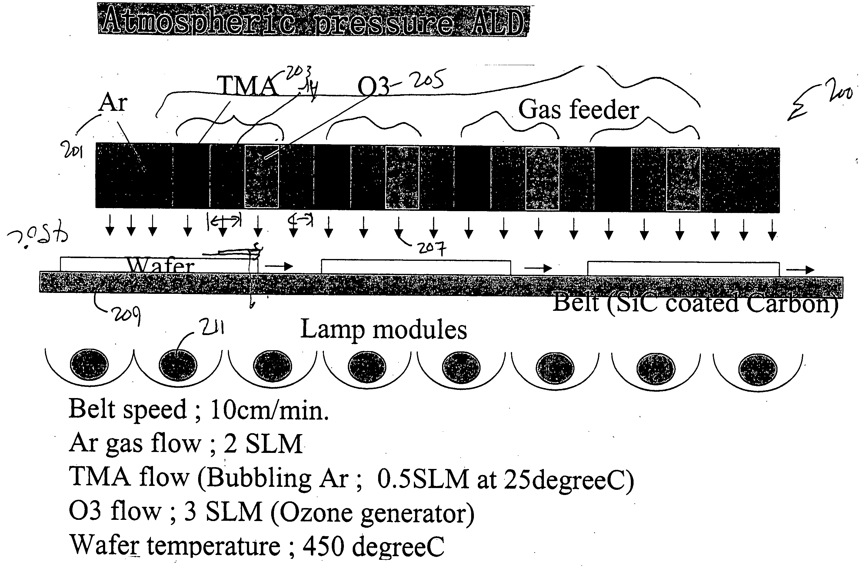
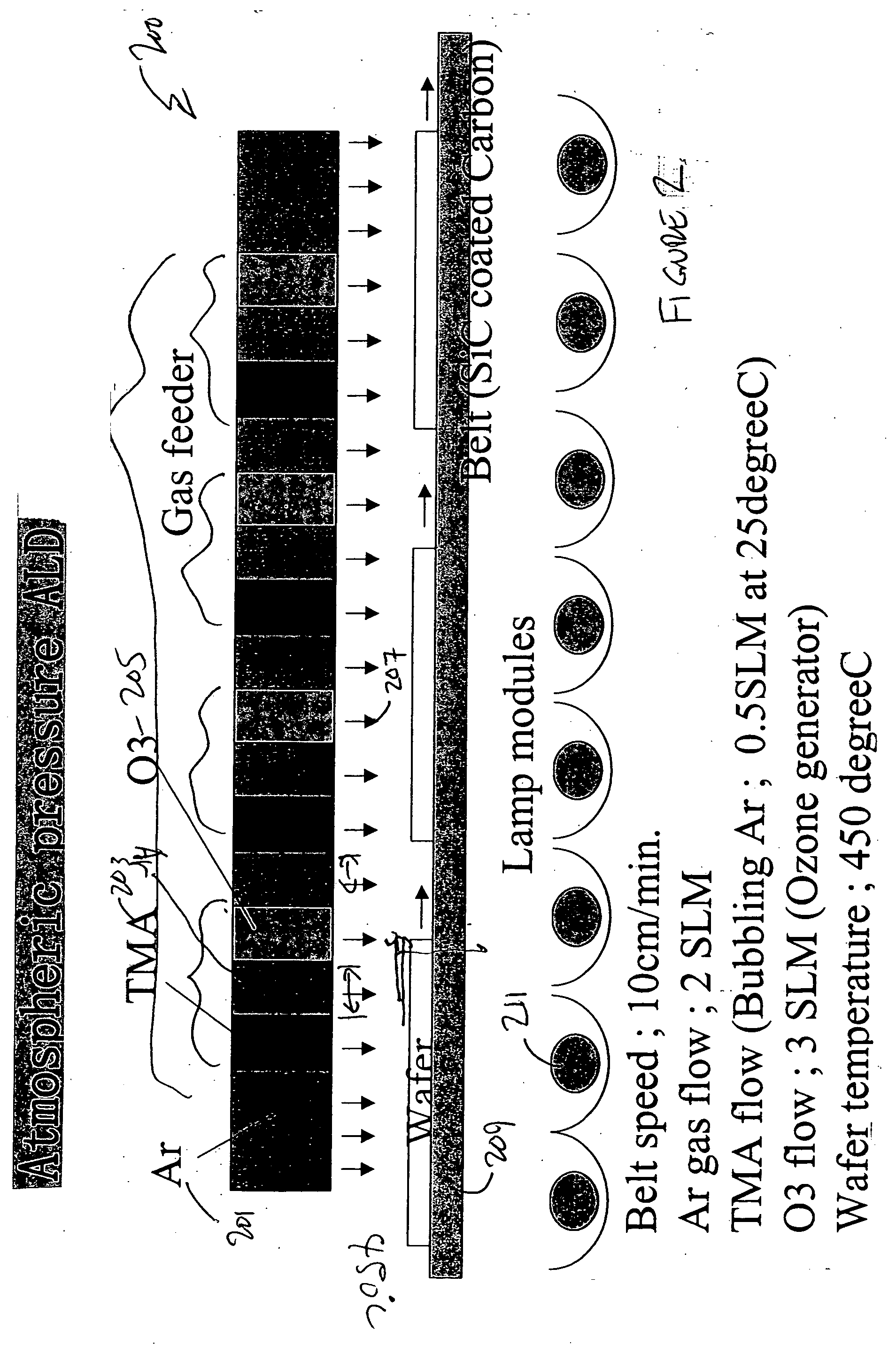
[0014] According to the present invention, techniques directed to integrated circuits and their processing for the manufacture of semiconductor devices are provided. More particularly, the invention provides a method and structures for depositing one or more films of materials using atomic layer deposition under atmospheric conditions. Merely by way of example, the invention has been applied to the manufacture of advanced integrated circuit devices, but it would be recognized that the invention has a much broader range of applicability.

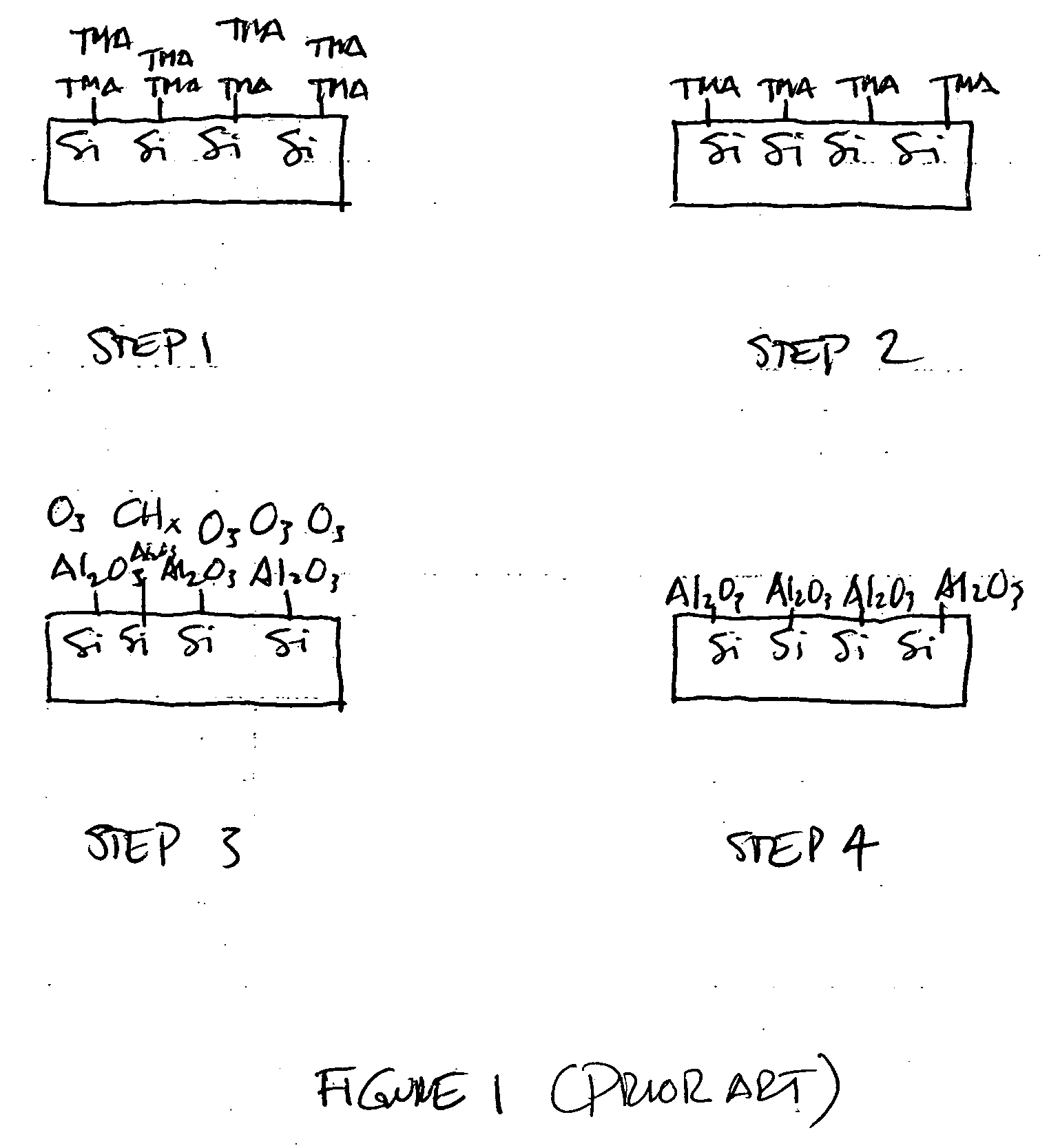
[0015]FIG. 1 is a simplified diagram illustrating a conventional method for atomic layer deposition. As shown, there are four main processes or steps in conventional atomic layer deposition. Step 1 includes a silicon substrate treated with Me3Al (TMA). The TMA is the metal precursor made using chemisorption. The method purges the TMA as illustrated in step 2. The method reacts the TMA with ozone to form aluminum oxide (Al2O3), which is a monolayer. O...


PUM

PropertyMeasurementUnit
aspect ratioaaaaaaaaaa
atmospheric pressureaaaaaaaaaa
temperatureaaaaaaaaaa

Abstract

A method for atomic layer deposition. The method includes providing a substrate having a surface region and exposing the surface region of the substrate to an atmospheric pressure. The method also maintains at least the substrate at about the atmospheric pressure and forms a film overlying the surface region using atomic layer deposition, while the substrate is maintained at about atmospheric pressure. Preferably, the film is grown at a rate of greater than about 1 nanometer per minute.

Description

BACKGROUND OF THE INVENTION [0001] The present invention is directed to integrated circuits and their processing for the manufacture of semiconductor devices. More particularly, the invention provides a method and structures for depositing one or more films of materials using atomic layer deposition under atmospheric conditions. Merely by way of example, the invention has been applied to the manufacture of advanced integrated circuit devices, but it would be recognized that the invention has a much broader range of applicability. [0002] Integrated circuits have evolved from a handful of interconnected devices fabricated on a single chip of silicon to millions of devices. Conventional integrated circuits provide performance and complexity far beyond what was originally imagined. In order to achieve improvements in complexity and circuit density (i.e., the number of devices capable of being packed onto a given chip area), the size of the smallest device feature, also known as the devi...

Claims


Application Information

Patent Timeline
Patent Type & Authority Applications(United States)
IPC IPC(8): C23C16/00
CPCC23C16/403C23C16/45525C23C16/45551
Inventor MIENO, FUMITAKE
Owner SEMICON MFG INT (SHANGHAI) CORP
Why Eureka
Try Eureka