Method of forming micro-patterns using multiple photolithography process

a photolithography and micro-pattern technology, applied in the field of micro-patterns, can solve the problems of inability to perform as a mask for subsequent etching processes, decreased device yield, and high cost of etching process

Inactive Publication Date: 2007-04-12
SAMSUNG ELECTRONICS CO LTD
View PDF1 Cites 20 Cited by
  • Summary
  • Abstract
  • Description
  • Claims
  • Application Information

AI Technical Summary

Benefits of technology

[0028] The present disclosure also provides a method of forming micro-patterns in which a flat anti-reflection layer can be formed without

Problems solved by technology

However, there are several drawbacks in the photolithography process.
That is, as defects between micro-patterns increase, such as, shorts, bridges, and pattern collapse, the yield of the devices decreases.
Further, as the thicknesses of photoresists (Tpr) used for patterning continuously decrease, the photoresist cannot perform as a mask for subsequent etching processes.
In addition, when the high numerical aperture is employed, there are problems in that the angle of incidence of light increases and the reflection ratio also increases.
In addition, as semiconductor devices become more highly integrated, light transmitted through a photo mask having adjacent micro-patterns is diffracted and interferes when an exposure process is performed, such that a uniform critical dimension (CD) for the patterns cannot be obtained.
However, in the conventional process of forming the second photores

Method used


Image

  • Method of forming micro-patterns using multiple photolithography process
  • Method of forming micro-patterns using multiple photolithography process
  • Method of forming micro-patterns using multiple photolithography process

Examples


Embodiment Construction

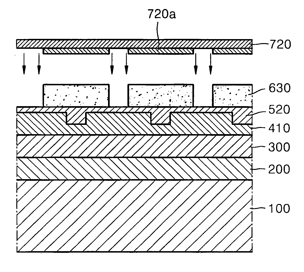
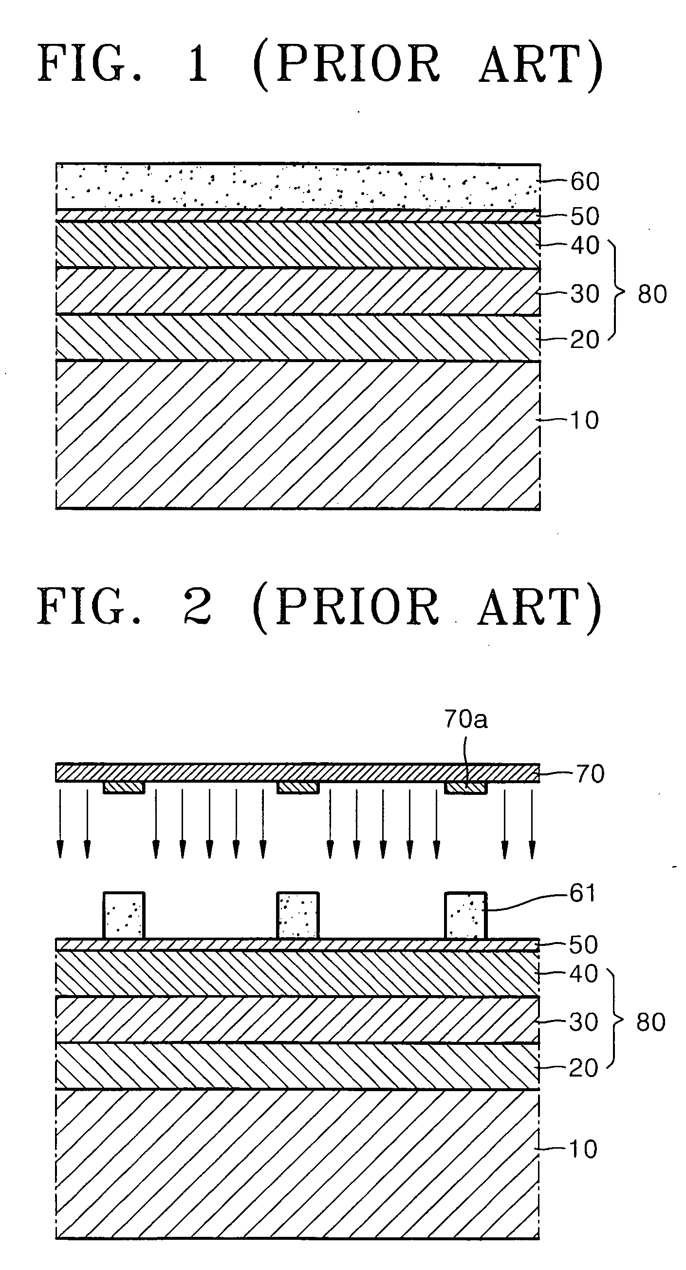
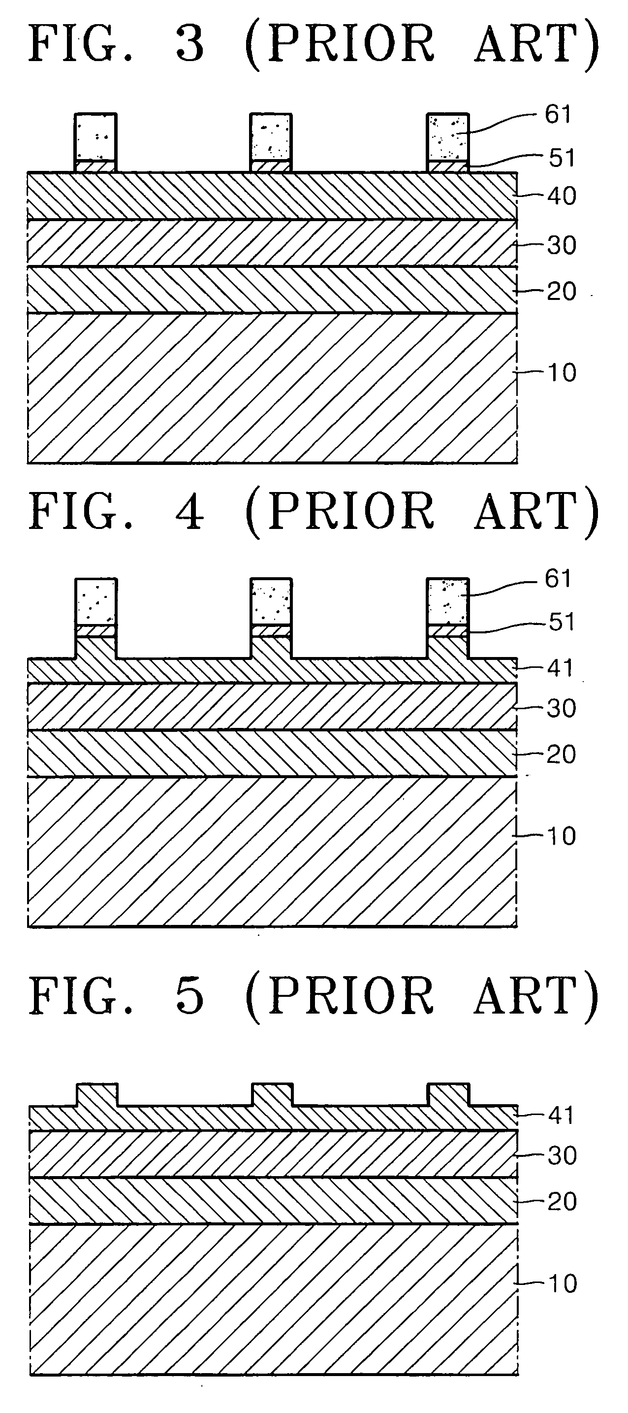
[0047] Hereinafter, embodiments in accordance with various aspects of the present disclosure will be described more fully with reference to the accompanying drawings, in which exemplary embodiments are shown. It will also be understood that when a layer is referred to as being “on” another layer or a substrate, it can be directly on the other layer or the substrate, or intervening layers can also be present. In any given layer or a substrate, there can be at least two surface levels formed in portions thereof, i.e., a higher level and a lower level. The higher level can be referred to as an “embossed” portion of the layer or substrate and the lower level can be referred to as an “engraved” portion of the layer or substrate. As an example, the engraved portion can be formed by etching and the embossed portions can be unetched. As used herein a “pattern” is a layer having at least one engraved portion, and can also be referred to as a “layer pattern.” In the drawings, like reference n...


PUM


Abstract

Provided is a method of forming micro-patterns using a multi-photolithography process, including: providing an etch target layer where micro-patterns are to be formed; forming a mask layer on the etch target layer; forming a first mask pattern including engraved portions and embossed portions by etching a predetermined region of the mask layer; forming a final mask pattern in the first mask pattern by etching a predetermined region of the residual embossed portions of the mask layer; and forming micro-patterns by etching the etch target layer using the final mask pattern as an etch mask.

Description

CROSS-REFERENCE TO RELATED PATENT APPLICATION [0001] This application claims priority to Korean Patent Application No. 10-2005-0095503, filed on Oct. 11, 2005, in the Korean Intellectual Property Office, the disclosure of which is incorporated herein in its entirety by reference. BACKGROUND OF THE INVENTION [0002] 1. Field of the Invention [0003] The present invention relates to a method of forming micro-patterns, and more particularly, to a method of forming micro-patterns using a multiple photolithography process. [0004] 2. Description of the Related Art [0005] A patterning process used for manufacturing a semiconductor device is a process of patterning a predetermined material layer formed on a wafer, and generally includes applying a photosensitive film, exposing the film, and developing the film, in that order. Relatively small patterns can be referred to as micro-patterns. [0006] When forming micro-patterns the most significant factor during the patterning process is resolutio...

Claims


Application Information

Patent Timeline
IPC IPC(8): G03C5/00
CPCG03F7/0035H01L21/0332H01L21/0337H01L21/3086H01L21/31144H01L21/32139
Inventor YANG, SONG-YICHI, KYEONG-KOO
Owner SAMSUNG ELECTRONICS CO LTD
Why Eureka
Try Eureka