Method of manufacturing contact hole

a contact hole and manufacturing method technology, applied in the direction of semiconductor/solid-state device manufacturing, basic electric elements, electric devices, etc., can solve the problems of increasing the difficulty of fabricating these devices, reducing the dimension and the width of interconnection lines linking up various devices, and reducing the size of the device. , to achieve the effect of increasing the ability to control the critical dimension

Inactive Publication Date: 2007-04-12
POWERCHIP SEMICON CORP
View PDF2 Cites 11 Cited by
  • Summary
  • Abstract
  • Description
  • Claims
  • Application Information

AI Technical Summary

Benefits of technology

[0008] Accordingly, at least one objective of the present invention is to provide a method of manufacturing contact hole that can increase the capability of controlling the critical dimension.

Problems solved by technology

With the rapid development of integrated circuit fabrication technologies, device miniaturization and integration is a definite trend and an important target issue for the manufacturing industry.
However, as the size of the devices continues to shrink, the dimension and the width of interconnecting lines linking up various devices also reduce.
Therefore, the process of fabricating these devices has become increasingly difficult.
For example, due to the size reduction, optical properties of material is harder to gauge and the photolithographic process has encountered some machine processing limits and physical limit in optical properties.
As a result, the process of fabricating contact holes using photolithographic technique is increasingly difficult and the critical dimension and the alignment accuracy of the contact hole are increasingly difficult to control.
Consequently, the cost of production continues to rise while the yield continues to drop.

Method used


Image

  • Method of manufacturing contact hole
  • Method of manufacturing contact hole
  • Method of manufacturing contact hole

Examples


Embodiment Construction

[0030] Reference will now be made in detail to the present preferred embodiments of the invention, examples of which are illustrated in the accompanying drawings. Wherever possible, the same reference numbers are used in the drawings and the description to refer to the same or like parts.

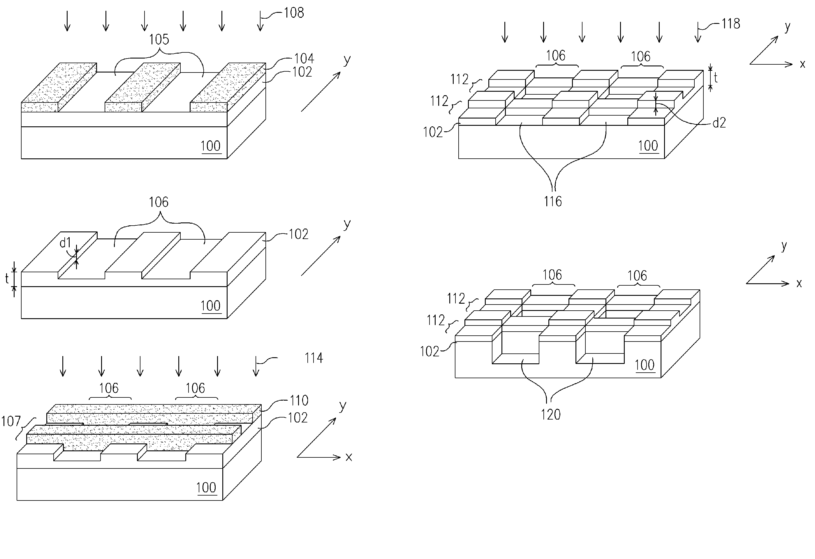
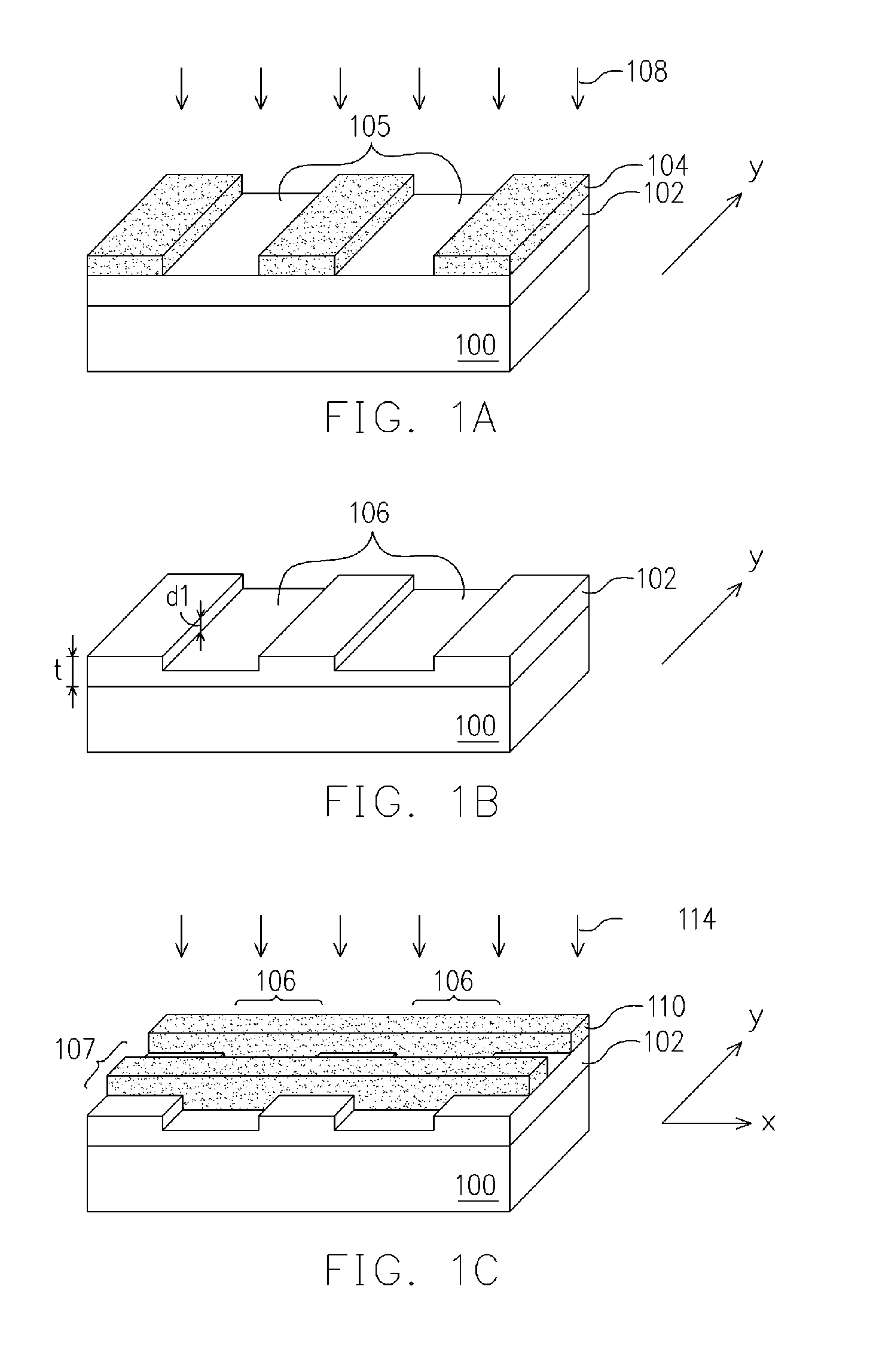
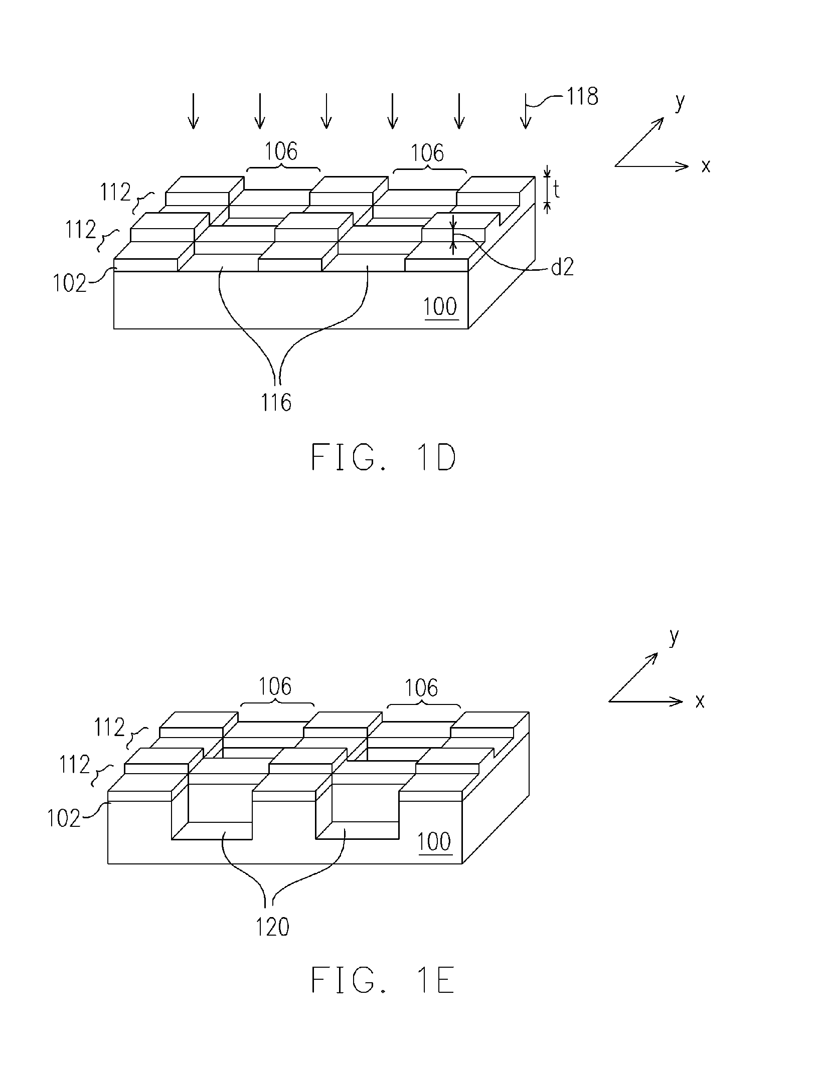
[0031]FIGS. 1A through 1E are perspective views showing the steps for fabricating contact holes on a substrate according to a first embodiment of the present invention. The term ‘contact hole’ is a generic term for all kinds of contact holes, via holes and other types having a similar structure.

[0032] First, as shown in FIG. 1A, a substrate 100 is provided. The substrate 100 has a semiconductor device or a metallic interconnect (not shown) disposed therein, for example. The uppermost layer is an inter-layer dielectric (ILD, not shown), for example. The contact will form in the inter-layer dielectric (ILD) layer so that the semiconductor device or the metallic interconnect can electrically connect ...


PUM


Abstract

A method of manufacturing contact hole is provided. First, a mask layer is formed on a substrate and a plurality of trenches is formed in the mask layer along two directions that cross over each other. The depth of the trenches is not greater than the thickness of the mask layer. However, there is an opening in the mask layer in the place where the trenches cross over each other. The opening exposes the substrate. Part of the substrate exposed by the opening is removed to form a contact hole in the substrate. In photolithography, it is easier to form lines than to form dots. Hence, the dimensions of contact holes are more precisely controlled.

Description

CROSS-REFERENCE TO RELATED APPLICATION [0001] This application claims the priority benefit of Taiwan application serial no. 94135336, filed on Oct. 11, 2005. All disclosure of the Taiwan application is incorporated herein by reference. BACKGROUND OF THE INVENTION [0002] 1. Field of the Invention [0003] The present invention relates to a method of manufacturing semiconductor device. More particularly, the present invention relates to a method of manufacturing contact hole that uses a mask. [0004] 2. Description of the Related Art [0005] With the rapid development of integrated circuit fabrication technologies, device miniaturization and integration is a definite trend and an important target issue for the manufacturing industry. However, as the size of the devices continues to shrink, the dimension and the width of interconnecting lines linking up various devices also reduce. Therefore, the process of fabricating these devices has become increasingly difficult. [0006] For example, du...

Claims


Application Information

Patent Timeline
Patent Type & Authority Applications(United States)
IPC IPC(8): H01L21/44
CPCH01L21/31144H01L21/76802
Inventor CHEN, KAO-TUNHSIAO, LI-TUNG
Owner POWERCHIP SEMICON CORP
Why Eureka
Try Eureka