Organometallic complex, and light-emitting element and light-emittting device using the same
a technology of organic complexes and light-emitting elements, applied in the field of substances, can solve the problems of limited element structure of ir complexes and poor heat resistance of ir complexes, and achieve the effect of superior heat resistan
- Summary
- Abstract
- Description
- Claims
- Application Information
AI Technical Summary
Benefits of technology
Problems solved by technology
Method used
Image

Examples
embodiment mode 1
(Embodiment Mode 1)
[0076] This embodiment mode will explain an organometallic complex of the present invention.
[0077] Organometallic complexes represented by structural formulas (6) to (84) can be given as one mode of the present invention. However, the present invention is not limited to the description here.
[0078] Each of the organometallic complexes of the present invention described above emits phosphorescence. Therefore, by using an organometallic complex of the present invention as a light-emitting substance, a light-emitting element having high internal quantum efficiency and luminous efficiency can be manufactured.
[0079] In addition, an organometallic complex generally has poor heat resistance. However, an organometallic complex of the present invention emits phosphoresce and is superior in heat resistance.
embodiment mode 2
(Embodiment Mode 2)
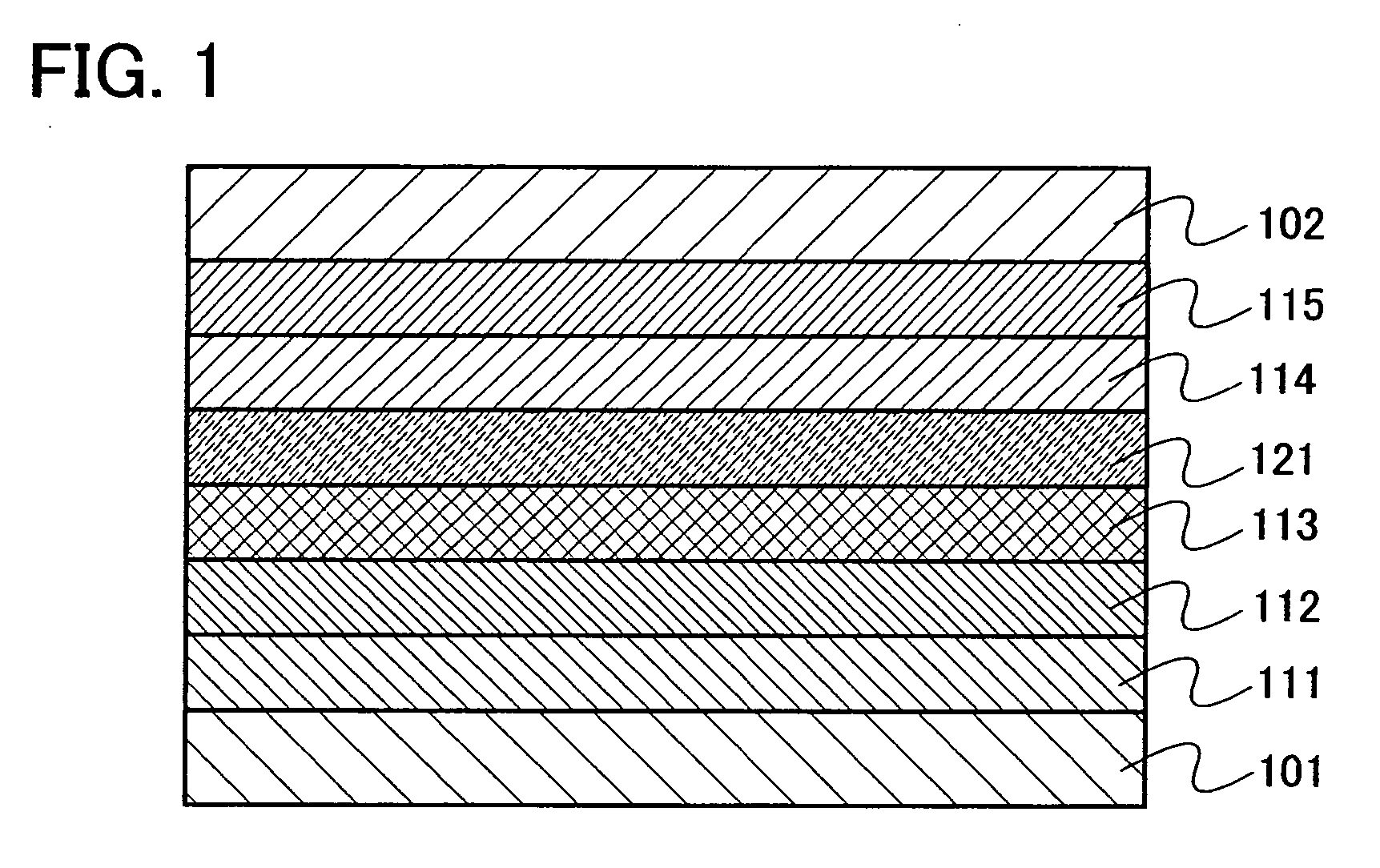
[0080] A mode of a light-emitting element in which an organometallic complex of the present invention is used as a light-emitting substance will be explained with reference to FIG. 1.
[0081]FIG. 1 shows a light-emitting element having a light-emitting layer 113 between a first electrode 101 and a second electrode 102. Then, the light-emitting layer 113 contains an organometallic complex according to the present invention having a structure represented by any of general formulas (G1), (G3), (G5), (G7), (G9), and (G11), or an organometallic complex according to the present invention represented by any of general formulas (G2), (G4), (G6), (G8), (G10), and (G12).
[0082] In addition to the light-emitting layer 113, a hole-injecting layer 111, a hole-transporting layer 112, an electron-transporting layer 114, an electron-injecting layer 115, a hole-blocking layer 121, or the like is provided between the first electrode 101 and the second electrode 102. These layers are...
embodiment mode 3
(Embodiment Mode 3)
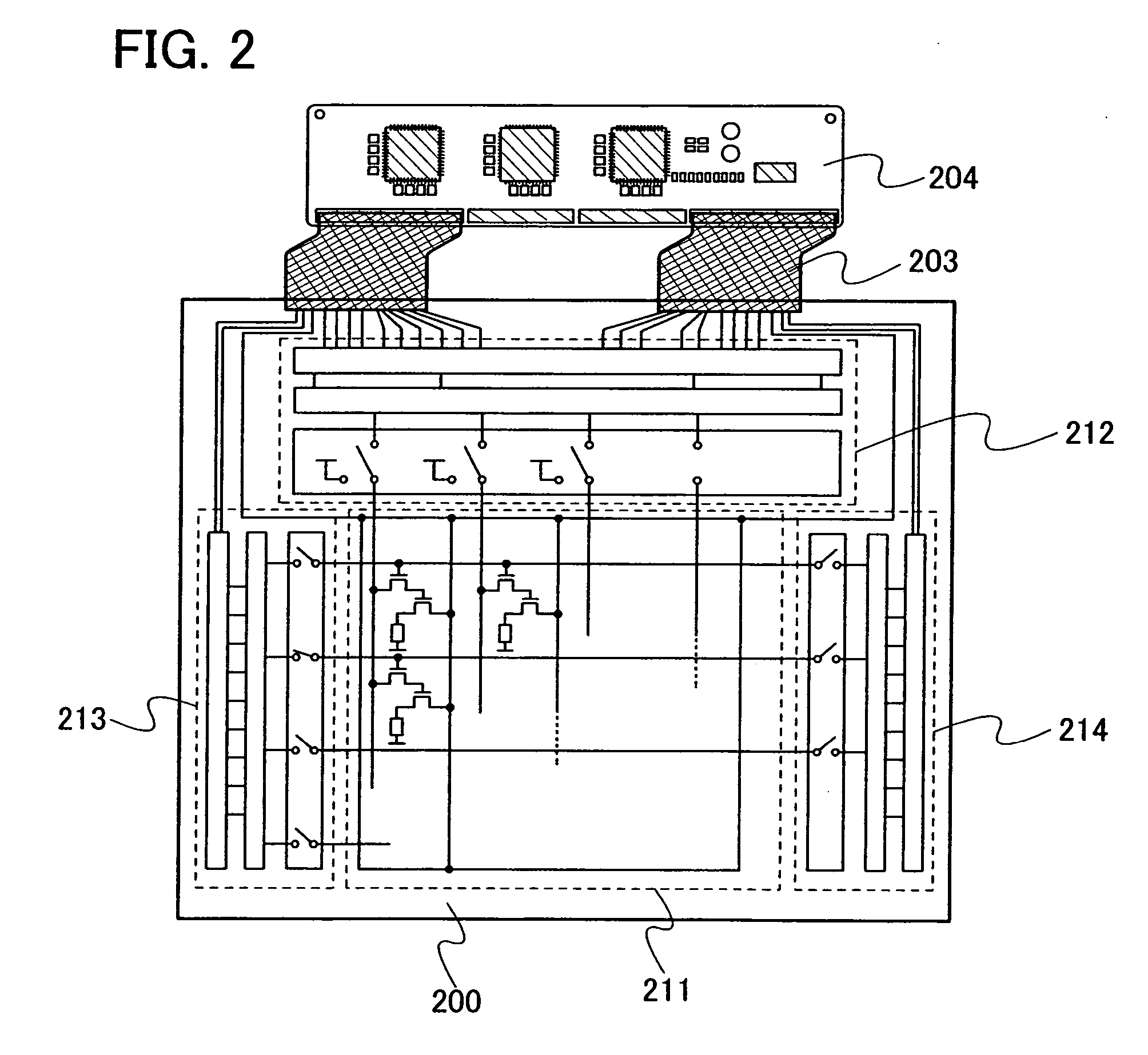
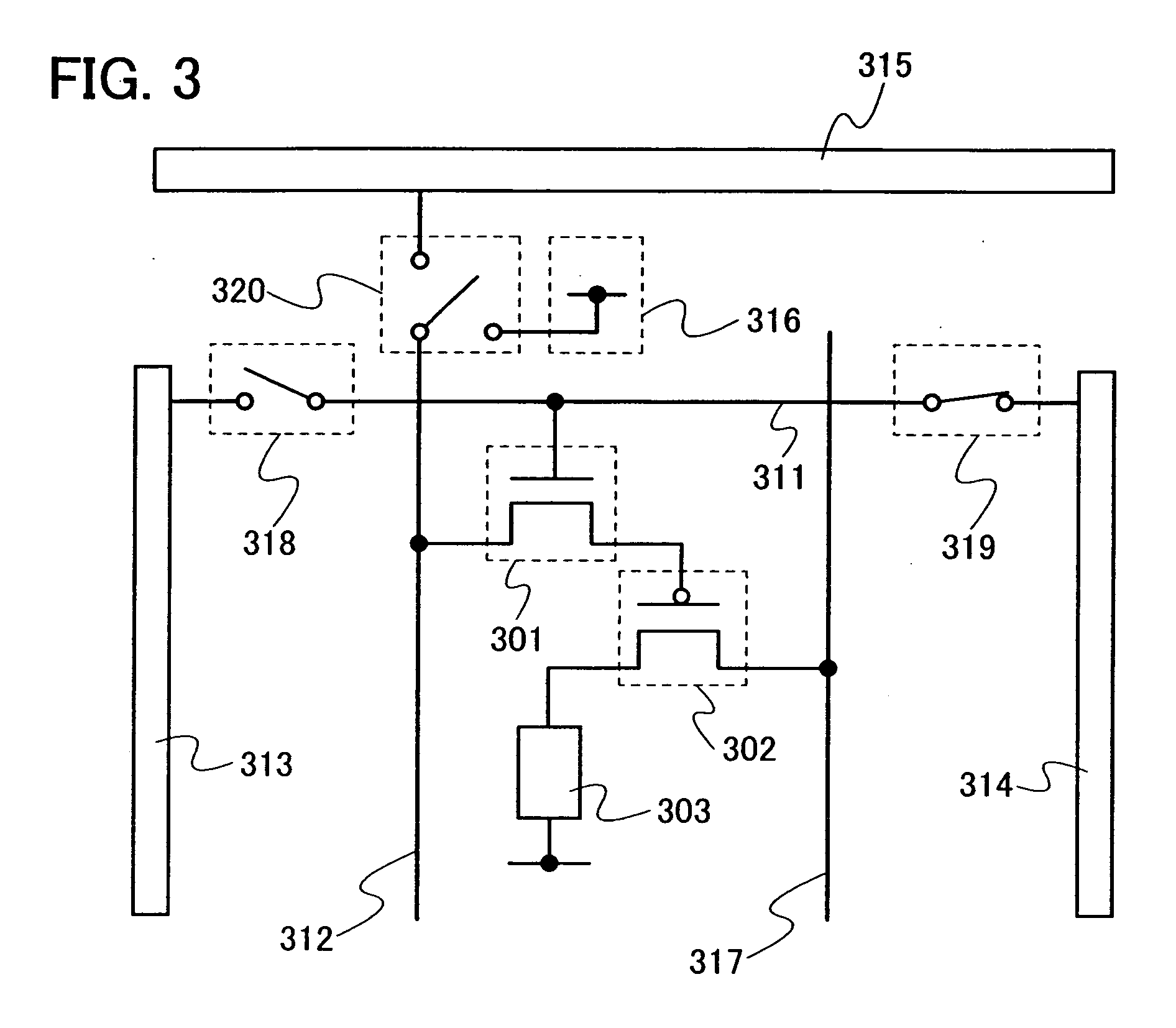
[0104] A light-emitting element according to the present invention using an organometallic complex according to the present invention as a light-emitting substance can emit light efficiently; therefore, light can be emitted with a few amount of current. Therefore, a light-emitting device according to the present invention using a light-emitting element according to the present invention as a pixel operates with low power consumption. This embodiment mode will explain a circuit configuration and a driving method of a light-emitting device having a display function with reference to FIGS. 2 to 5.
[0105]FIG. 2 is an overhead schematic view of a light-emitting device according to this embodiment mode. In FIG. 2, a pixel portion 211, a signal line driver circuit 212, a writing scanning line driver circuit 213, and an erasing scanning line driver circuit 214 are provided over a substrate 200. Each of the signal line driver circuit 212, the writing scanning line driver c...
PUM
| Property | Measurement | Unit |
|---|---|---|
| thickness | aaaaa | aaaaa |
| wavenumber | aaaaa | aaaaa |
| emission peak | aaaaa | aaaaa |
Abstract
Description
Claims
Application Information
 - R&D Engineer
- R&D Manager
- IP Professional
- Industry Leading Data Capabilities
- Powerful AI technology
- Patent DNA Extraction
Browse by: Latest US Patents, China's latest patents, Technical Efficacy Thesaurus, Application Domain, Technology Topic.
© 2024 PatSnap. All rights reserved.Legal|Privacy policy|Modern Slavery Act Transparency Statement|Sitemap