Active matrix driving display device and method of manufacturing the same

a technology of active matrix and driving display device, which is applied in the direction of organic semiconductor devices, semiconductor devices, instruments, etc., can solve the problems of difficult to make the active matrix driving display device large and to perform the manufacturing itself, and the plastic substrate may be easily deformed, so as to reduce the thermal deformation of the plastic substrate and increase the effect of safety

Inactive Publication Date: 2007-04-19
ELECTRONICS & TELECOMM RES INST
View PDF2 Cites 10 Cited by
  • Summary
  • Abstract
  • Description
  • Claims
  • Application Information

AI Technical Summary

Benefits of technology

[0013] The present invention is directed to an active matrix driving display device capable of reducing thermal deformation of a plastic substrate and protecting the plastic substrate to increase safety and a method of manufacturing the same.

Problems solved by technology

However, when an active matrix driving display device is manufactured using a glass substrate, since the glass substrate is relatively heavy and fragile, it is difficult to make the active matrix driving display device large as well as to perform the manufacturing itself.
However, when the active layer is formed by the lithography employing relatively high energy, the plastic substrate may be easily deformed due to the high thermal energy, and therefore it is difficult to form the active layer.
However, since leakage may occur through ends of the gate electrode, it is difficult to effectively drive the active matrix driving display device.

Method used


Image

  • Active matrix driving display device and method of manufacturing the same
  • Active matrix driving display device and method of manufacturing the same
  • Active matrix driving display device and method of manufacturing the same

Examples


Embodiment Construction

[0026] A method of manufacturing an active matrix driving display device of the present invention will now be described more fully hereinafter with reference to the accompanying drawings, in which preferred embodiments of the invention are shown.

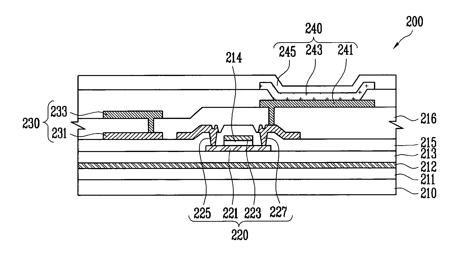
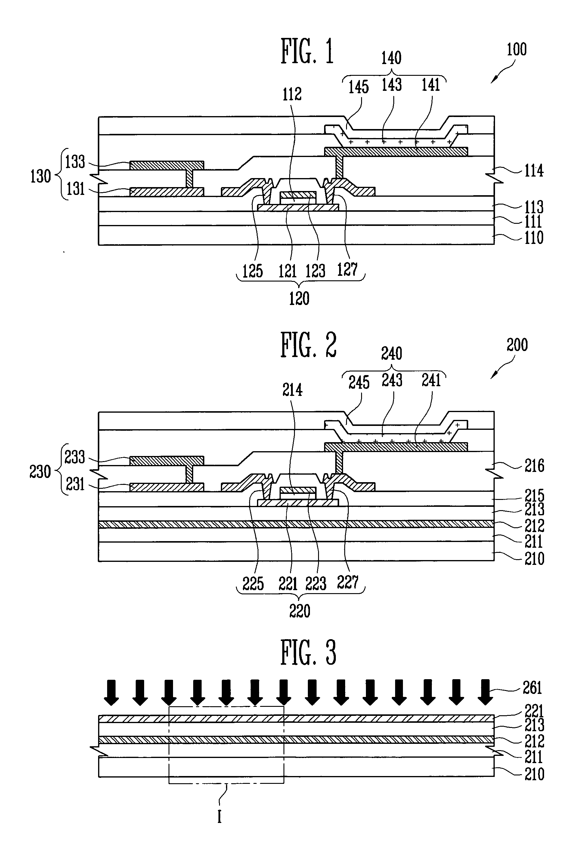
[0027]FIG. 2 is a partial cross-sectional view of an active matrix driving display device in accordance with an embodiment of the present invention. Referring to FIG. 2, the active matrix driving display device 200 includes a plastic substrate 210, a thin film transistor 220, a capacitor 230, and an organic light emitting diode 240. The thin film transistor 220 is formed on the plastic substrate 210, and includes an active layer 221, a gate electrode 223, a source electrode 224, and a drain electrode 227. The capacitor 230 is composed of a pair of electrodes 231 and 233, and the organic light emitting diode 240 is electrically connected to the thin film transistor 220, and includes a pixel electrode 241, an organic emission layer 243, and a...


PUM


Abstract

Provided are an active matrix driving display device and a method of manufacturing the same. The active matrix driving display device includes: a first buffer layer formed on a plastic substrate; a laser-absorbing layer formed on the first buffer layer; a second buffer layer formed on the laser-absorbing layer; and an active layer formed on the second buffer layer, whereby it is possible to prevent deformation of the plastic substrate even when light or heat is used during the formation of the active layer.

Description

CROSS-REFERENCE TO RELATED APPLICATION [0001] This application claims priority to and the benefit of Korean Patent Application No. 2005-96772, filed on Oct. 14, 2005, the disclosure of which is incorporated herein by reference in its entirety. BACKGROUND [0002] 1. Field of the Invention [0003] The present invention relates to an active matrix driving display device and a method of manufacturing the same, and more particularly, to an active matrix driving display device manufactured using a plastic substrate and a method of manufacturing the same. [0004] 2. Discussion of Related Art [0005]FIG. 1 is a partial cross-sectional view of an active matrix driving display device formed on a glass substrate. Referring to FIG. 1, the active matrix driving display device 100 includes a substrate 110, a thin film transistor 120 having an active layer 121 (referred to as so called “semiconductor layer”) formed on the substrate 110, a capacitor 130, and a light emitting diode 140. The substrate 11...

Claims


Application Information

Patent Timeline
Patent Type & Authority Applications(United States)
IPC IPC(8): H01L31/12
CPCG02F1/133305G02F1/1362H01L27/12H01L27/3244H01L27/1281H01L51/52H01L51/5237H01L2251/5338H01L29/78603H10K59/12H10K50/80H10K50/844H10K2102/311H10K59/87G02F1/136H10K50/84
Inventor KIM, YONG HAECHUNG, CHOONG HEUILEE, JIN HO
Owner ELECTRONICS & TELECOMM RES INST
Why Eureka
Try Eureka