Optical connection structure of optical backplane to circuit substrate

a technology of optical backplane and circuit substrate, which is applied in the direction of optical light guides, fibre transmission, instruments, etc., can solve the problems of limited transmission speed of electric substrate used in equipment, drawback to the increase of equipment capacity, and difficulty in attaching connectors, so as to increase the density of mounting the circuit substrate to the optical backplane

Inactive Publication Date: 2007-04-19
NEC CORP +3
View PDF2 Cites 61 Cited by
  • Summary
  • Abstract
  • Description
  • Claims
  • Application Information

AI Technical Summary

Benefits of technology

[0024] According to the present invention, the mounting density of the circuit substrate to the optical backplane can be increased.

Problems solved by technology

However, the limit of transmission speed of an electric substrate used in the equipment acts as a drawback to the increase of the capacity of the equipment.
This is because when the optical fibers are laid to overlap a portion where a connector is attached, it is difficult to attach the connector.
A disadvantage arises here in that the optical fibers have a lower limit in a bending radius.
Because of the above reasons, the structure of the conventional optical backplane has a disadvantage in that the mounting density of the optical backplane cannot be increased due to necessity of bypassing the connector portion when the optical fibers are laid and to the lower limit of the fiber-bending radius.

Method used


Image

  • Optical connection structure of optical backplane to circuit substrate
  • Optical connection structure of optical backplane to circuit substrate
  • Optical connection structure of optical backplane to circuit substrate

Examples


first embodiment

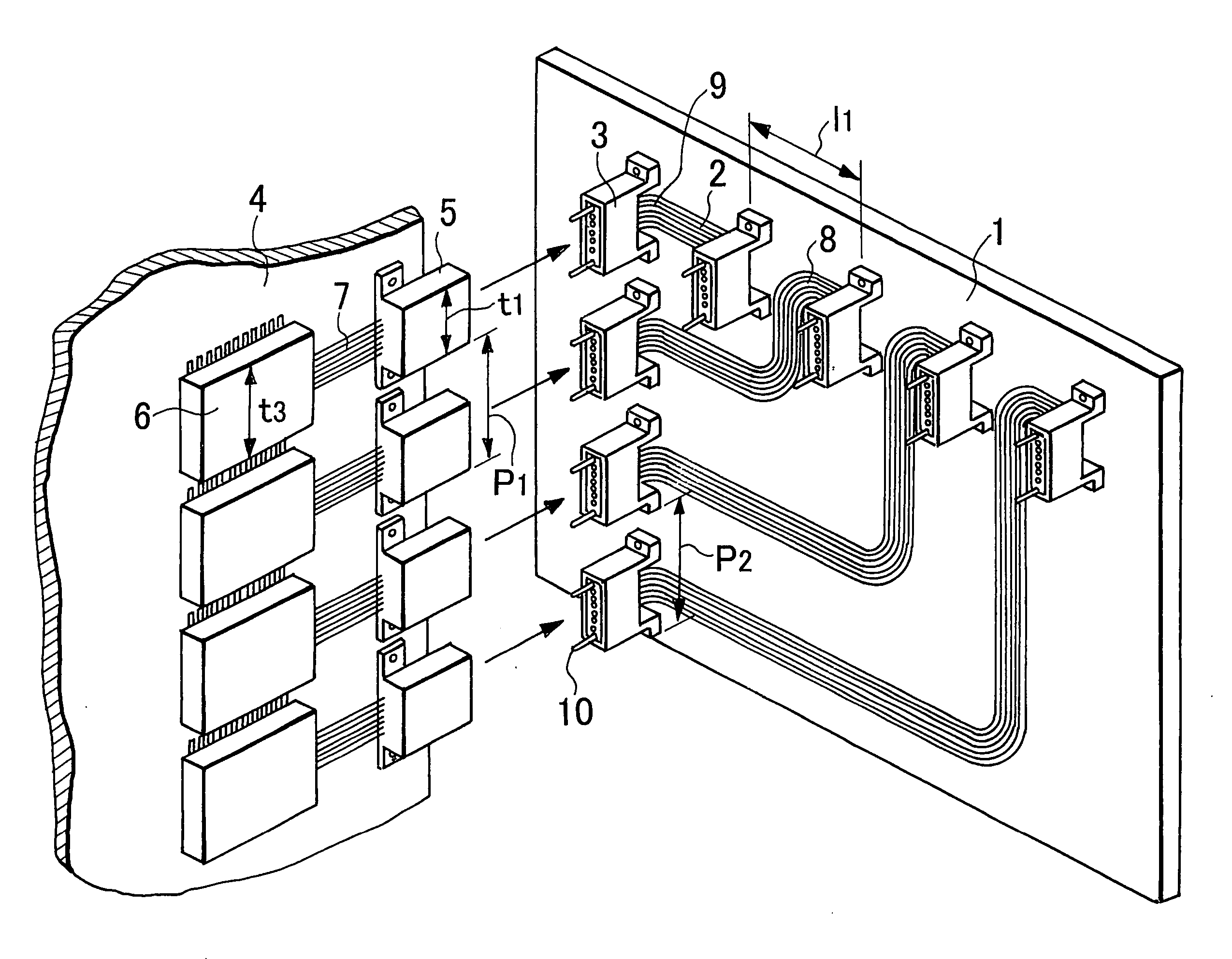
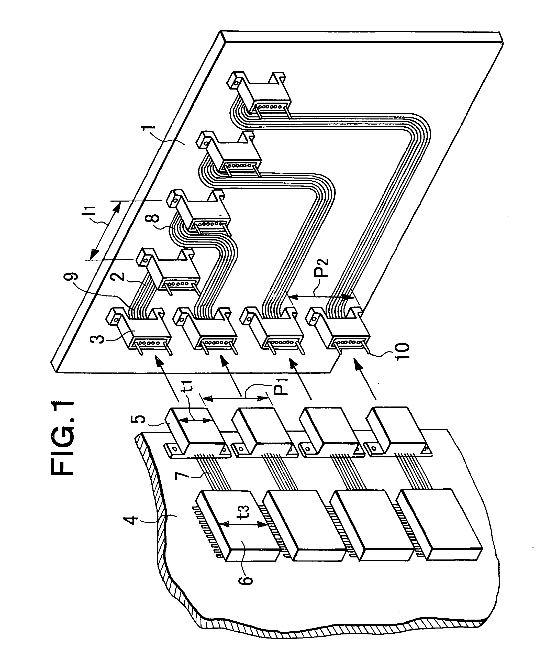
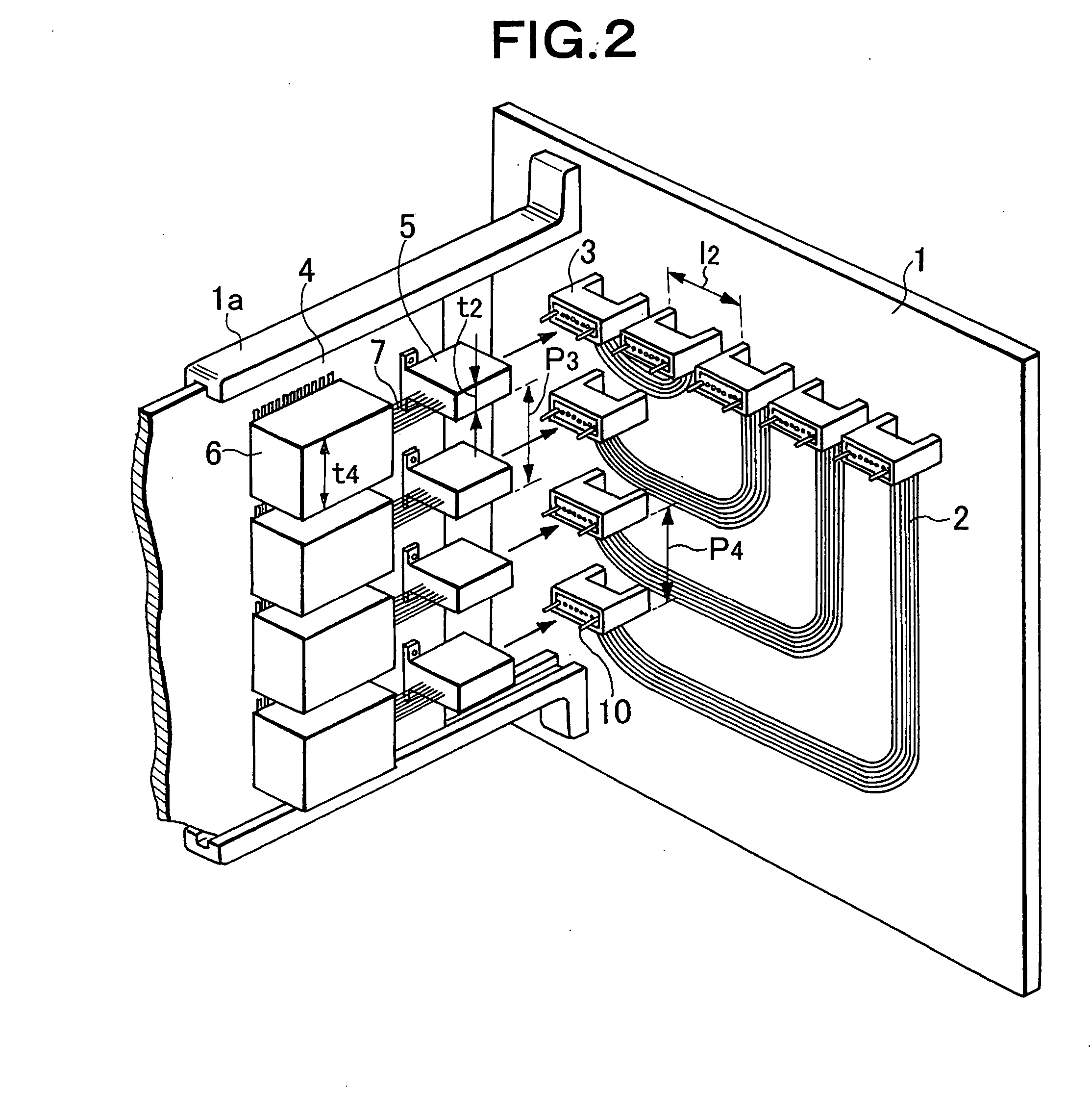
[0042]FIG. 2 is a perspective view showing a connecting portion between a circuit substrate and the optical backplane of a first embodiment according to the present invention in information processing equipment. FIG. 5 is a perspective view showing an overall arrangement of the information processing equipment.

[0043] As shown in FIG. 5, in the information processing equipment, a plurality of circuit substrates 4 are accommodated in a cabinet 31, and the plurality of circuit substrates 4 are disposed to an optical backplane 1 at about right angles. Optical connectors 5 and photoelectric conversion modules 6 on the circuit substrates side are disposed on the circuit substrates 4, and optical connectors 3 on the optical backplane side are disposed to the optical backplane 1. The optical connectors 3 are optically connected to the optical connectors 5. There are, for example, a router, a server, and the like as the information processing equipment according to the first embodiment.

[00...

second embodiment

[0058]FIGS. 7A to 7C are views showing a connecting portion of a circuit substrate and optical backplane of a second embodiment of the present invention in the information processing equipment. FIG. 7A is an exploded sectional view of an arrangement of the third embodiment when viewed from the upper surface of a board, FIG. 7B is a view when viewed from the front surface of an optical backplane, and FIG. 7C is a sectional view of a state that the board is inserted into the optical backplane when viewed from the upper surface of the board.

[0059] An overall arrangement of the information processing equipment of the third embodiment is different from the first embodiment in that no photoelectric conversion module is mounted on the circuit substrate, an electric connector is disposed on the circuit substrate, an photoelectric conversion module is disposed in an electric connector on the optical backplane, and the photoelectric conversion module is directly connected to an optical conne...

third embodiment

[0084]FIG. 16 is a perspective view showing a connecting portion between a circuit substrate and the optical backplane in a third embodiment of the present invention in information processing equipment. In FIG. 16, the same components as those of FIGS. 2 and 15 are denoted by the same reference numeral, and the explanation thereof is omitted.

[0085] In the third embodiment, optical connectors 3-1 are disposed in about parallel to the main surface of a board 4 and optical connectors 3-2 are disposed at about a right angle to the main surface of the board 4. The disposing direction of the optical fibers of the optical connectors 3-1 is in about parallel to the main surface of a board 4 in the same way as the optical connectors 3 of FIG. 1. The disposing direction of the optical fibers of the optical connectors 3-2 is in nonparallel (here, at about a right angle) to the main surface of a board 4 in the same way as the optical connectors 3 of FIG. 2.

[0086] Five boards are attached to t...


PUM


Abstract

An optical backplane includes an optical connector which receives juxtaposed optical signals transmitted in nonparallel to the main surface of a circuit substrate from the circuit substrate or transmits juxtaposed optical signals in nonparallel to the main surface of the circuit substrate to the circuit substrate. The optical connector disposes and accommodates edge portions of a plurality of optical fibers and the disposing direction of the optical fibers in the optical connector is in nonparallel to the main surface of the circuit substrate.

Description

BACKGROUND OF THE INVENTION [0001] 1. Field of the Invention [0002] The present invention relates to an optical backplane for carrying out signal connection between a plurality of circuit substrates (boards), which are mounted in information processing equipment such as a router, a server, or the like, by optical signals, and to a light transmission method. [0003] 2. Description of the Related Art [0004] Recently, as a broadband network expands, an amount of information distributed through the network is increased. Consequently, it is required to increase the information processing capacity of information processing equipment such as a router, a server or the like. However, the limit of transmission speed of an electric substrate used in the equipment acts as a drawback to the increase of the capacity of the equipment. To further increase the information processing capacity of the information processing equipment by overcoming the drawback, it is effective to connect between boards ...

Claims


Application Information

Patent Timeline
Patent Type & Authority Applications(United States)
IPC IPC(8): G02B6/00G02B6/38G02B6/42H04B10/25H04B10/80
CPCG02B6/3897G02B6/43
Inventor SASAKI, JUNICHIKURATA, KAZUHIKOSUZUKI, SHUJISAITO, KAZUHITOMASUDA, HIROSHIIBARAGI, OSAMUKINOSHITA, MASAO
Owner NEC CORP
Why Eureka
Try Eureka