Current sensor
- Summary
- Abstract
- Description
- Claims
- Application Information
AI Technical Summary
Benefits of technology
Problems solved by technology
Method used
Image
Examples
first embodiment
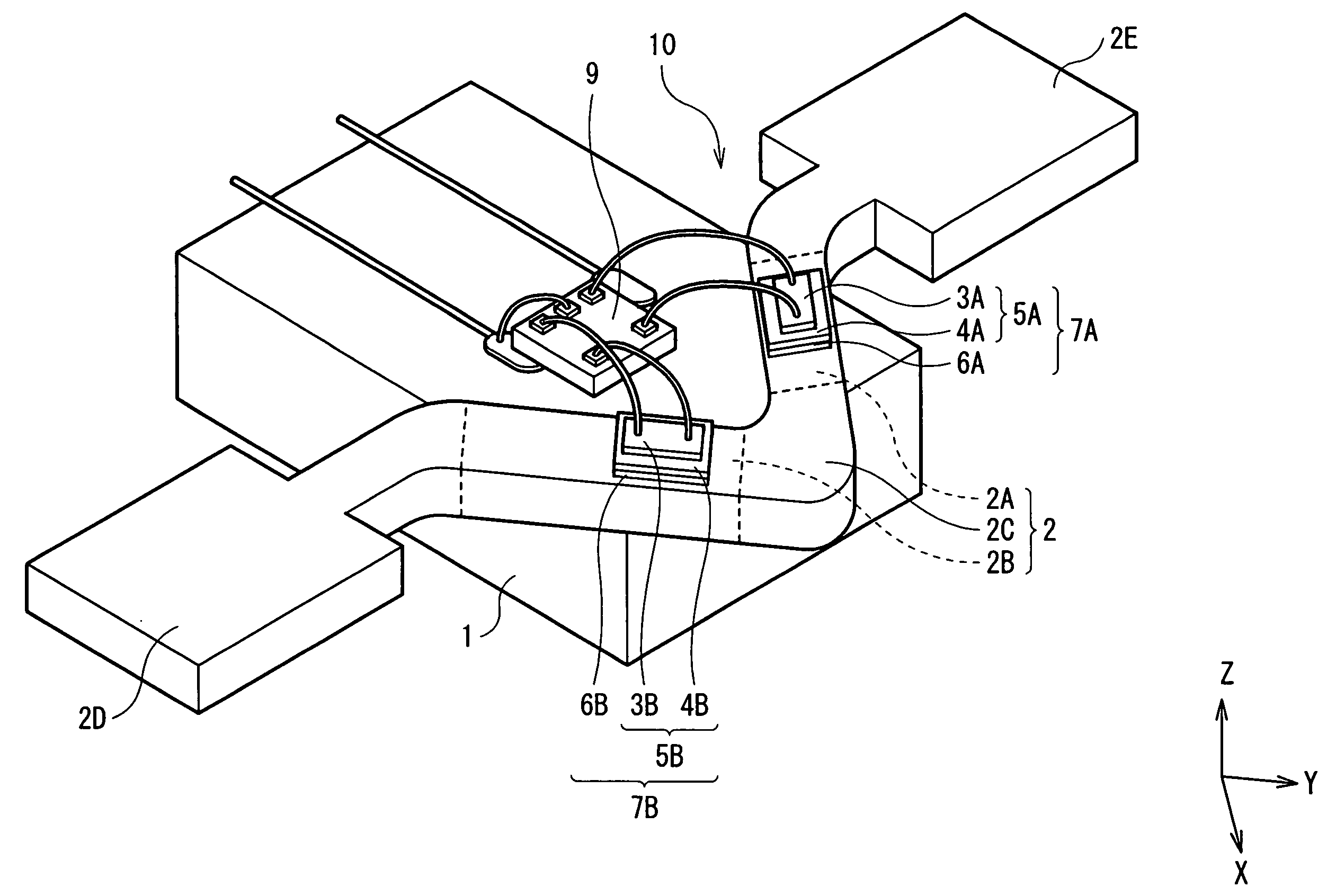
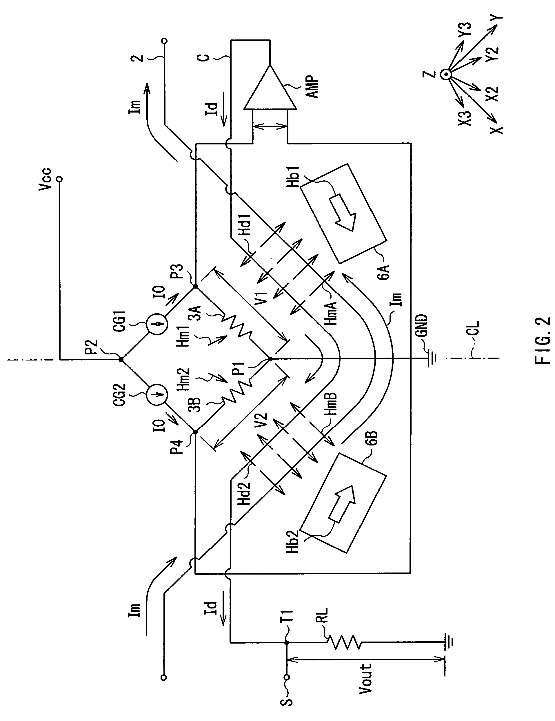
[0043] First, a configuration of a current sensor according to a first embodiment in the present invention will be explained with reference to FIG. 1 and FIG. 2. FIG. 1 is a schematic diagram showing a perspective configuration of a current sensor 10 according to the present embodiment, and FIG. 2 expresses a circuit configuration of the current sensor 10 appearing in FIG. 1. Directions of all the arrows representing a current to be detected Im, a compensating current Id, current magnetic fields HmA and HmB, compensating current magnetic fields Hd, bias magnetic fields Hb1 and Hb2, and a current I0 indicate a relative direction with respect to a first and a second magnetoresistive elements 3A and 3B (which will be described later) in FIG. 2.
[0044] The current sensor 10 is an ammeter for measuring the current to be detected Im supplied to a conductor line 2 formed on a substrate 1, and is provided with magnetic sensors 7A and 7B including the first and the second magnetoresistive el...
first modification
[0075] Herein, a modification of the current sensor according to the present embodiment will be explained with reference to FIGS. 9A and 9B.
[0076] As shown in FIGS. 4A and 4B, the current sensor according to the foregoing first embodiment is configured so that the magnetization directions J13A and J13B of the free layers 13 are orthogonal to the magnetization directions J11A and J11B of the pinned layers 11 when no external magnetic field H is applied. However in the present invention, as shown in the modification shown in FIGS. 9 A and 9B, the current sensor may also be configured in such a way that magnetization directions J13A0 and J13B0 of the free layers 13 are parallel to the magnetization directions J11A and J11B of the pinned layers 11, respectively when no external magnetic field H is applied. Specifically, in FIG. 9A, the magnetization direction J11A and the magnetization direction J13A0 of the MR element 3A are both in the +X3 direction orthogonal to the synthetic magnet...
second embodiment
[0079] A current sensor as a second embodiment according to the present invention will be explained next. Although in the foregoing first embodiment is explained the case in which the conductor line 2 having V-shaped configuration (in plan view) is used, in the second embodiment is explained a case in which a straight-line shaped conductor line 21 is employed.
[0080] Since the current sensor of the second embodiment has substantially the same configuration as that of the above-mentioned first embodiment except for the conductor line 21, here is explained the relation among the magnetization directions J11 and J13 of the GMR films in the MR elements 3A and 3B, the bias magnetic field Hb, and the current magnetic field Hm with reference to FIGS. 11A and 11B. FIGS. 11A and 11B are conceptual diagrams about the relation among the current direction, the magnetic field direction, and the magnetization direction according to the current sensor of the second embodiment. Here, a current to b...
PUM
 Abstract
Description
Claims
Application Information


