Transistor circuit, pixel circuit, display device, and driving method therefor

a technology of transistor circuit and display device, which is applied in the direction of static indicating device, pulse technique, instruments, etc., can solve the problems of transistor circuit malfunction, deterioration of light-emission element brightness, and inability to maintain constant threshold voltage vth of thin-film transistors,

Active Publication Date: 2007-04-26
JOLED INC
View PDF10 Cites 55 Cited by
  • Summary
  • Abstract
  • Description
  • Claims
  • Application Information

AI Technical Summary

Benefits of technology

[0006] In view of the above-described known technical problems, an object of the present invention is to provide a transistor circuit having the function of correcting variations in the threshold voltage of a thin-film transistor, a pixel circuit, a display device, and a driving method therefor. For achieving the object, the following means is provided. That is to say, a transistor circuit having a plurality of thin-film transistors formed on a substrate and wiring adapted to connect a gate, a source, and / or a drain of each of the thin-film transistors, so as to perform a predetermined operation, is provided. The transistor circuit includes at least one thin-film transistor applied with a forward bias between a gate and a source repeatedly and / or continuously via wiring during the operation, and reverse-bias-application means configured to suppress a variation in a threshold voltage of the thin-film transistor by applying a reverse bias between the gate and source of the thin-film transistor in such timing that the operation is not disturbed.
[0011] Further, the present invention provides a display device including scan lines in rows, scan lines in columns, and pixel circuits provided at intersections of the scan lines, wherein, upon being selected by the scan line, the pixel circuit samples a video signal from the signal line and drives a light-emission element according to the sampled video signal. The pixel circuit includes a plurality of thin-film transistors formed on a substrate, wiring adapted to connect a gate, a source, and / or a drain of each of the thin-film transistors, at least one thin-film transistor applied with a forward bias between a gate and a source repeatedly and / or continuously via wiring while the light-emission element is driven, and reverse-bias-application means configured to suppress a variation in a threshold voltage of the thin-film transistor by applying a reverse bias between the gate and source of the thin-film transistor in such timing that the driven light-emission element is not disturbed.
[0014] Further, the present invention provides a method of driving a transistor circuit including a plurality of thin-film transistors formed on a substrate and wiring adapted to connect a gate, a source, and / or a drain of each of the thin-film transistors, so as to perform a predetermined operation. The driving method is adapted to perform a forward bias-application step adapted to apply a forward bias between the gate and the source of at least one of the thin film transistors repeatedly and / or continuously via the wiring during the operation, and a reverse bias-application step adapted to suppress a variation in a threshold voltage of the thin-film transistor by applying a reverse bias between the gate and source of the thin-film transistor in such timing that the operation is not disturbed. Further, a complement step is included, the complement step being adapted to drive an additional thin-film transistor connected in parallel to the thin-film transistor complementarily relative to the thin-film transistor, thereby generating timing where the operation is not disturbed, wherein the reverse bias-application step is adapted to apply the reverse bias to the thin-film transistor in the generated timing.

Problems solved by technology

However, the threshold voltage Vth of the thin-film transistor is not necessarily constant but varied with time.
Due to the variation in the threshold voltage, the cut-off operation is disturbed, which causes the transistor circuit to malfunction.
In the case of a pixel circuit configured to drive a light-emission element by a current, the drain current is varied due to the variation in the threshold voltage, so that the brightness of the light-emission element is deteriorated.

Method used


Image

  • Transistor circuit, pixel circuit, display device, and driving method therefor
  • Transistor circuit, pixel circuit, display device, and driving method therefor
  • Transistor circuit, pixel circuit, display device, and driving method therefor

Examples


Embodiment Construction

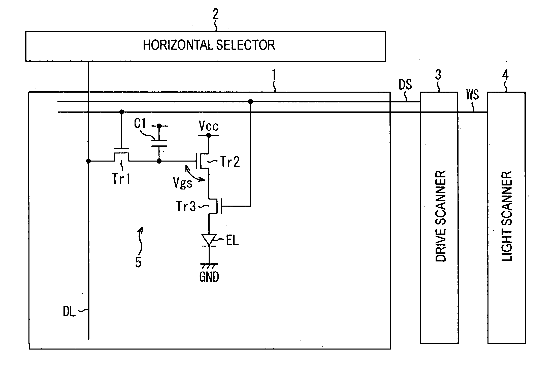
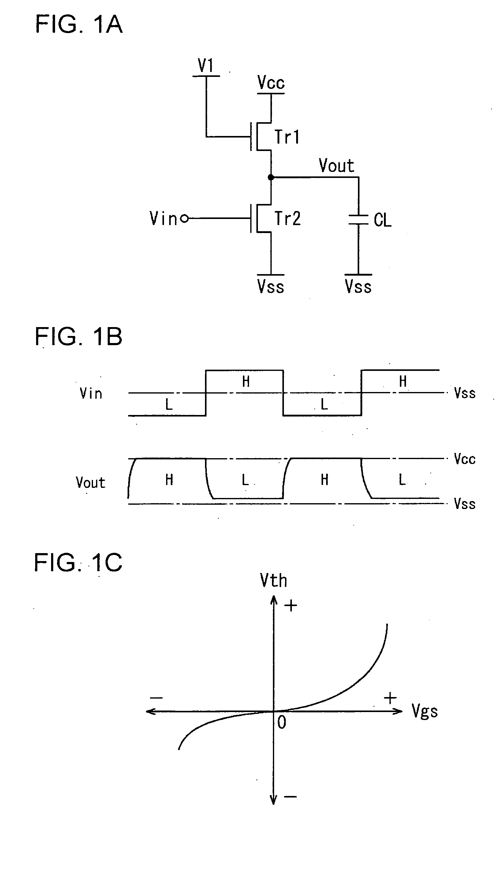
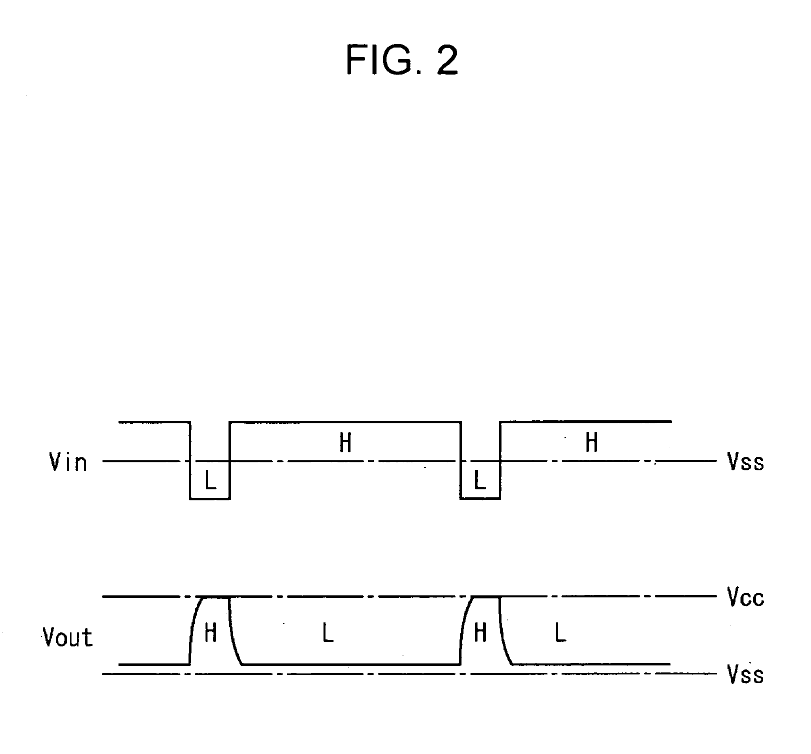
[0029] Hereinafter, embodiments of the present invention will be described in detail with reference to the attached drawings. FIGS. 1A to 1C show a transistor circuit according to a first embodiment of the present invention. FIG. 1A is a circuit diagram showing the structure, FIG. 1B is a timing chart showing the operations, and FIG. 1C is a graph showing the principles. As shown in FIGS. 1A, the transistor circuit includes two thin-film transistors Tr1 and Tr2 formed on a substrate, and wiring provided for connecting the gates, sources, and drains of the thin-film transistors Tr1 and Tr2, so as to perform inverter operations. That is to say, the transistor circuit is forms an inverter by using two N-channel transistors Tr1 and Tr2. Since the N-channel thin-film transistor can be produced at low cost by using an amorphous silicon film, as an active layer, the N-channel thin-film transistor has a cost advantage. Here, the inverter is shown, as merely an example, and it is essential o...


PUM

PropertyMeasurementUnit
threshold voltageaaaaaaaaaa
voltageaaaaaaaaaa
drain current Idsaaaaaaaaaa

Abstract

A transistor circuit having the function of correcting variations in the threshold voltage of a thin-film transistor is provided. The transistor circuit includes a plurality of thin-film transistors (Tr1 to Tr3) formed on a substrate and wiring which connects the gate, source, and / or drain of each of the transistors, so as to perform a predetermined operation. During the operation, a forward bias is applied between the gate and source of the thin-film transistor (Tr2) via the wiring repeatedly and / or continuously. A reverse bias is applied between the gate and source of the transistor (Tr2) in such timing that the operation is not disturbed so that the variations in the threshold voltage are suppressed. More specifically, an additional transistor (Tr3) connected in parallel to the transistor (Tr2) is driven complementarily, so as to generate the above-described timing where the operation is not disturbed, and the reverse bias is applied to the transistor (Tr2) in the generated timing.

Description

TECHNICAL FIELD [0001] The present invention relates to a transistor circuit including thin-film transistors integrally formed on a substrate. Further, the present invention relates to a pixel circuit which is an example of the transistor circuit. Still further, the present invention relates to a display device including the pixel circuits arranged in matrix. The active-matrix display device includes a flat display panel such as a liquid-crystal display and an organic EL display, for example. BACKGROUND ART [0002] The thin-film transistor which is an example field-effect transistor uses an amorphous silicon film and / or a polycrystalline silicon film formed on an insulation substrate including glass or the like, as an element region. In recent years, the thin-film transistor has been actively developed, as a pixel switch of the active-matrix display device. The thin-film transistor includes a gate, a drain, and a source, and passes a current between the source and the drain according...

Claims


Application Information

Patent Timeline
Patent Type & Authority Applications(United States)
IPC IPC(8): G09G3/30G02F1/133G09G3/20G09G3/32H01L27/12H01L51/50H03K19/003H05B33/14
CPCG09G3/3233G09G2300/0819G09G2300/0852H03K19/00384G09G2310/0254G09G2320/043H01L27/12G09G2300/0861G02F1/133G09G3/20G09G3/30G09G3/32
Inventor UCHINO, KATSUHIDEYAMASHITA, JUNICHI
Owner JOLED INC
Why Eureka
Try Eureka