Imaging device

a technology of imaging device and lens, which is applied in the field of imaging device, can solve the problems of large aberration, large volume, and insufficient downsizing of imaging system having lens and solid-state imaging sensor such as ccd or cmos, and achieve the effects of suppressing the occurrence of stray light, small light loss, and high quality

Inactive Publication Date: 2007-04-26
PANASONIC CORP
View PDF5 Cites 78 Cited by
  • Summary
  • Abstract
  • Description
  • Claims
  • Application Information

AI Technical Summary

Benefits of technology

[0035] According to the present invention, it is possible to provide an imaging device which, in each imaging unit, is small in light loss, is operable to suppress an occurrence of a stray light, and is operable to provide an image with a high quality as far as a periphery thereof.
[0036] Also, according to the present invention, it is possible to provide an imaging device in which, in each imaging unit, a light from a micro lens can enter a photo-electric conversion element without shading, and thus enabling to provide a high quality image.

Problems solved by technology

However, imaging systems having lenses and solid-state imaging sensors such as a CCD or a CMOS are not yet sufficiently downsized, and there has been a demand for a development of a compact imaging system for realizing a camera with further portability.
Conventional optical systems having a plurality of lenses arranged along an optical axis have problems that their volumes become large due to their lengths extending along the optical axis, and that aberrations thereof are large due to large lens diameters.
However, according to the imaging system of patent document 1, resolution of an optical image of an object formed on an image flat surface is determined by the number and density of micro lenses (namely, pinholes), and therefore, obtaining a high quality image has been difficult.
However, due to limitation in downsizing of a micro lens, achieving a high resolution has been difficult.
Also, a luminous flux reaching an image flat surface is limited by pinholes thereby losing a large quantity of light, and thus a problem in terms of sensitivity has been caused.
With this imaging system, a quality of a shot image obtained from an imaging unit is low due to the small number of pixels included in each imaging unit.

Method used


Image

  • Imaging device
  • Imaging device
  • Imaging device

Examples


embodiment 1

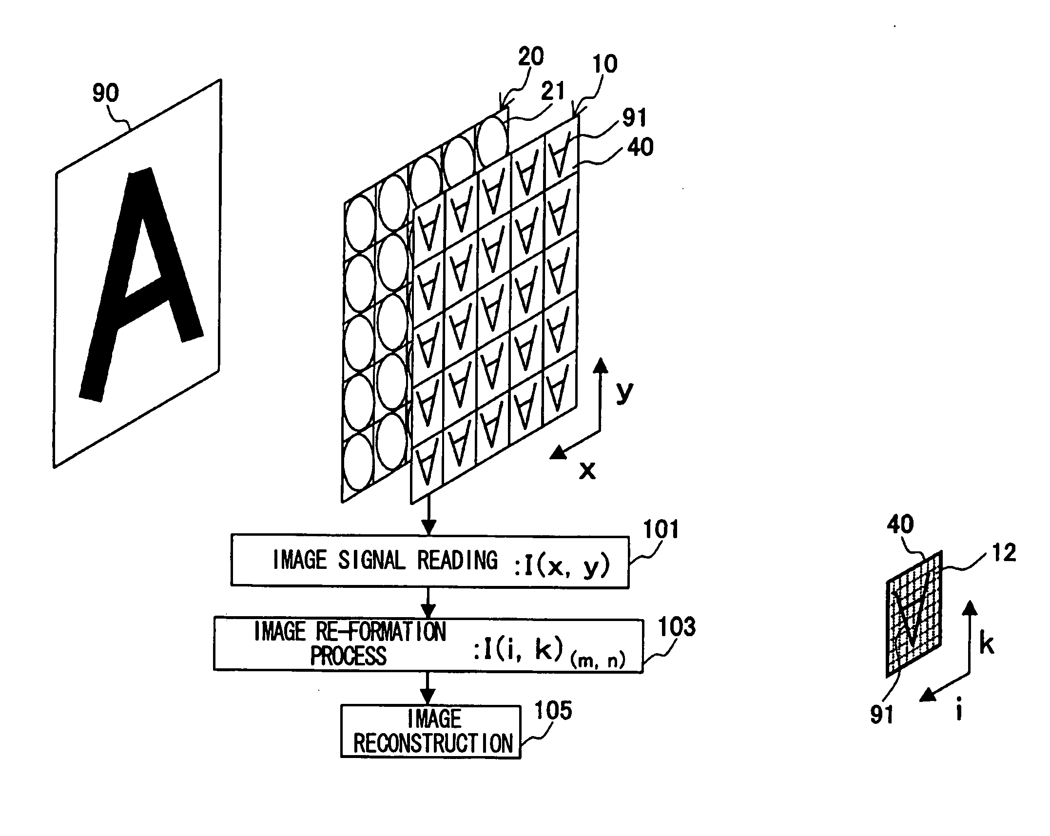
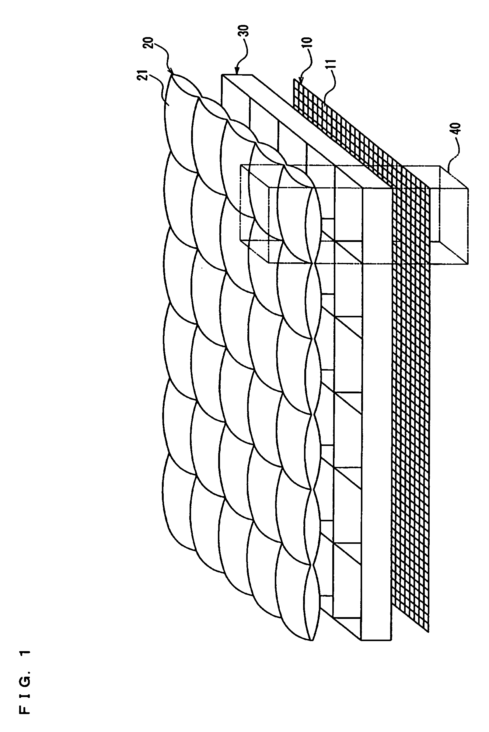
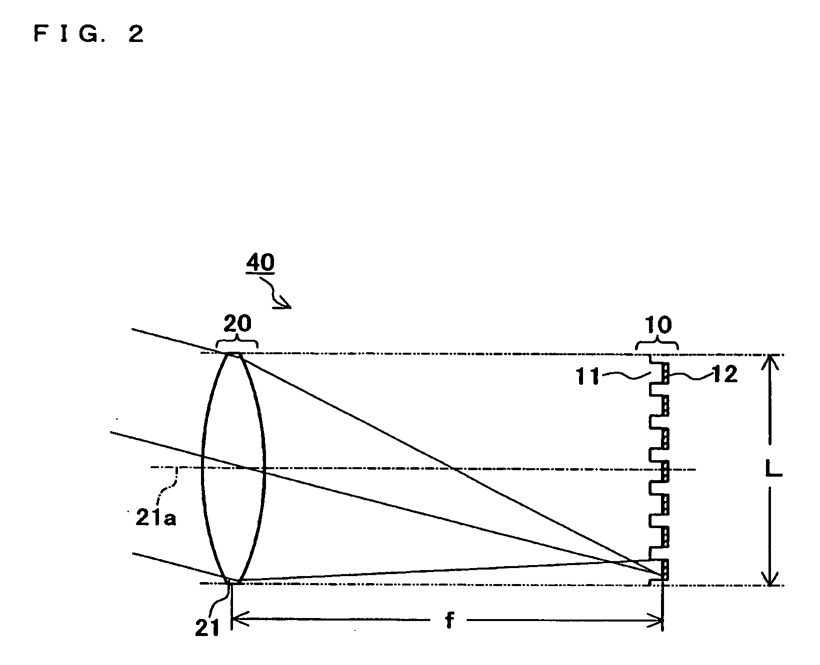
[0076]FIG. 1 is a diagrammatic perspective illustration showing a schematic configuration of an imaging device according to Embodiment 1 of the present invention. In FIG. 1, the imaging device comprises a solid-state imaging sensor 10 (e.g., CCD or CMOS) including a large number of pixels 11 two dimensionally arranged in lateral and longitudinal directions on a first flat surface, and a micro lens array 20 including a plurality of micro lenses 21 two dimensionally arranged in lateral and longitudinal directions on a second flat surface separately provided so as to be parallel to the first flat surface. The solid-state imaging sensor 10 includes an imaging area of unit including a plurality of the pixels 11, and each micro lens forms an optical image of an object on a corresponding imaging area of unit. In other words, a luminous flux from the object enters the plurality of micro lenses 21, and each of the micro lenses 21 forms an optical image of the object on a corresponding imagin...

embodiment 2

[0091] An imaging device according to Embodiment 2 of the present invention is described focusing on differences from Embodiment 1. FIG. 5 is a cross sectional illustration of the imaging unit 40 of the imaging device according to the present embodiment showing a section including the optical axis 21a of the micro lens 21. The present embodiment differs from Embodiment 1 in that a pixel lens 13 is provided on a light incidence side of the light receiving section 12 of the solid-state imaging sensor 10 so as to have one on one correspondence between the light receiving section 12 and the pixel lens 13. Elements having a function similar to that in Embodiment 1 are attached with same reference numerals as in Embodiment 1, and a description therefor is omitted.

[0092] The pixel lens 13 is also referred to as an “on chip lens”, and leads a luminous flux which is to form an image on a place other than the light receiving section 12 to the light receiving section 12. Pitch in arranging pi...

embodiment 3

[0099] An imaging device according to Embodiment 3 of the present invention is described focusing on differences from Embodiments 1 and 2. FIG. 7 is a cross sectional illustration of the imaging unit 40 of the imaging device according to the present embodiment showing a section including the optical axis 21a of the micro lens 21. In the present embodiment, a pixel lens 14 is provided on the light incidence side of the light receiving section 12 of the solid-state imaging sensor 10 so as to have one on one correspondence between the light receiving section 12 and the pixel lens 14, as in Embodiment 2. However, the present embodiment differs from Embodiment 2 in that at least one of pixel lenses 14 is positioned such that an optical axis thereof is displaced from the center of the corresponding light receiving section 12, whereas optical axes of all the pixel lenses 13 pass through centers of the corresponding light receiving sections 12 in Embodiment 2. It is not necessary that the a...


PUM


Abstract

There is provided an imaging device which is small in light loss, is operable to suppress an occurrence of a stray light, and is operable to provide an image with a high quality as far as a periphery thereof. The imaging device operable to output an image of an object as an electrical image signal, comprising: a solid-state imaging sensor including pixels which are two dimensionally arranged on a first flat surface and each of which has a photo-electric conversion function; and a lens array including micro lenses two dimensionally arranged on a second flat surface separately provided so as to be parallel to the first flat surface, in which the solid-state imaging sensor includes an imaging area of unit including a plurality of pixels, and each of the micro lenses forms an optical image of the object on a corresponding imaging area of unit and satisfies a predetermined condition, arctan(L/f)≦θ, for a pixel, from among pixels included in an imaging area of unit corresponding to each micro lens, positioned farthest from an optical axis of a corresponding micro lens. Here, θ is a maximum angle of an incident light capable of entering a pixel, f is a focal length of a micro lens, and L is a diameter of a circle circumscribing an imaging area of unit corresponding to one of the micro lenses.

Description

[0001] This application is the U.S. National Phase under 35 U.S.C. § 371 of International Application No. PCT / JP2004 / 016332, filed Nov. 4, 2004, which in turn claims the benefit of Japanese Application No. 2003-374724, filed Nov. 4, 2003 and Japanese Application No. 2004-194195, filed Jun. 30, 2004, the disclosures of which Applications are incorporated by reference herein in their entirety.TECHNICAL FIELD [0002] The present invention relates to an imaging device. Particularly, the present invention relates to an imaging device having a micro lens array including a plurality of micro lenses arranged on an object side of a solid-state imaging sensor including a large number of pixels. BACKGROUND ART [0003] There have been increasing needs for a compact, thin type camera with excellent portability in a digital still camera market recently expanding. Circuitry parts for a signal process such as an LSI are becoming ever functionally sophisticated and downsized by means of minute wiring ...

Claims


Application Information

Patent Timeline
Patent Type & Authority Applications(United States)
IPC IPC(8): H04N5/225G02B3/00G02B27/00H04N5/335
CPCG02B3/0056G02B27/0018H04N5/2254H04N23/55
Inventor OKAYAMA, HIROAKIYAMAGATA, MICHIHIROBOKU, KAZUTAKETANAKA, YASUHIROHAYASHI, KENICHIFUSHIMI, YOSHIMAMURATA, SHIGEKIHAYASHI, TAKAYUKI
Owner PANASONIC CORP
Why Eureka
Try Eureka