Standard cell

a technology of standard cell and layout design, applied in the field of standard cell, can solve the problems of low degree of layout design freedom, low degree of design freedom in the layout design of a standard cell itself, etc., and achieve the effect of simple wiring state, improved degree of freedom of layout design for a standard cell, and high degree of freedom of layout design

Inactive Publication Date: 2007-05-03
PANASONIC CORP
View PDF4 Cites 37 Cited by
  • Summary
  • Abstract
  • Description
  • Claims
  • Application Information

AI Technical Summary

Benefits of technology

[0061] Thus, according to the present invention, although the standard cell has a substrate power supply wire, the substrate power supply wire does not extend across the standard cell in the width direction, so that an empty region occurs, and therefore, a metal wire of the same layer can be disposed in this region. Thereby, the degree of freedom of layout design for a standard cell can be improved.
[0062] In addition, when a semiconductor integrated circuit is designed by disposing other standard cells adjacent to the standard cell, an inter-cell substrate power supply wire is not formed only by disposing the adjacent cells, and it is necessary to additionally dispose inter-cell substrate power supply wires connecting substrate power supply wires in a plurality of standard cells individually. In this case, the wiring route of the inter-cell substrate power supply wire can be freely set and changed so that crosstalk does not occur between a signal wire already disposed and the inter-cell substrate power supply wire, resulting in a high degree of freedom of layout design for a semiconductor integrated circuit.
[0063] In addition, since a normal power supply wire is previously fixedly disposed in a standard cell, when a semiconductor integrated circuit is designed, inter-cell normal power supply wires do not need to be disposed individually. Therefore, wide wires (normal power supply wires) do not need to be disposed individually, so that the wide wires and fine wires are not mixed in the wiring step, and therefore, a simpler wiring state should be taken into consideration in the wiring step, so that a design step can be completed in a shorter time.

Problems solved by technology

However, the first conventional example has a low degree of design freedom, and the second conventional example has a large number of design steps.
Firstly, the low degree of design freedom which is a problem with the first conventional example will be hereinafter described in detail in terms of two points.
Due to the design constraint, there is a problem that the degree of freedom of layout of metal wires is low in layout design of a standard cell itself.
Due to the design constraint, there is a problem that the degree of freedom of wiring is low in layout design of a semiconductor integrated circuit.
In addition, an influence of noise occurring in the victim due to the charge amount change ΔQ increases with a decrease in the current drive performance of the current supply source for driving the victim.
As a result, an operation of the transistor is affected.
In this case, a signal propagation speed of a propagation route via the transistor changes, so that timing violation is likely to occur.
As a result, a failure in signal transfer on a route having timing violation causes an incorrect operation of the semiconductor integrated circuit to be likely to occur, leading to a reduction in manufacturing yield.
However, the inter-cell substrate power supply wire 2503 is previously fixedly disposed in the standard cell 2500, so that the wiring route cannot be changed.
Thus, in the semiconductor integrated circuit employing the standard cell of the first conventional example, since the substrate power supply wire 15 is previously fixed, the degree of freedom of design is low, and the option of changing wiring is limited as described above.

Method used


Image

  • Standard cell
  • Standard cell
  • Standard cell

Examples


first example

[0080] Hereinafter, examples of the present invention will be described with reference to the drawings.

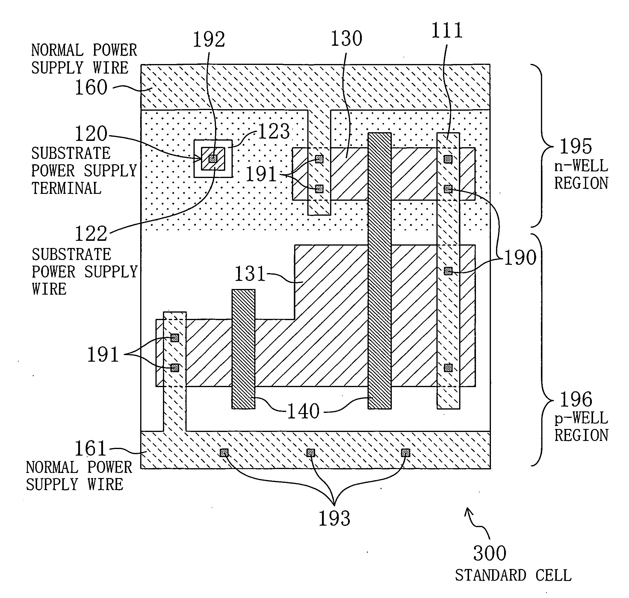
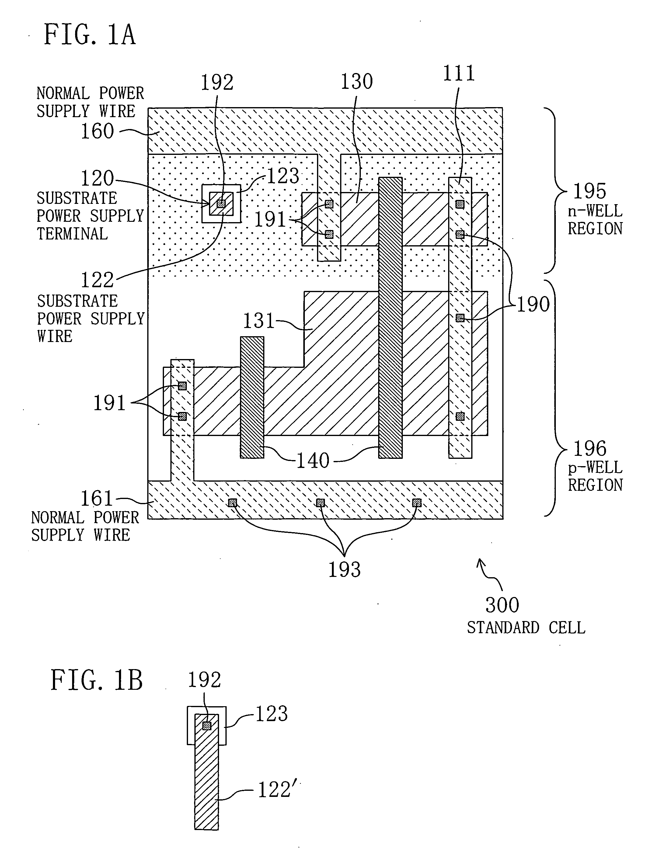
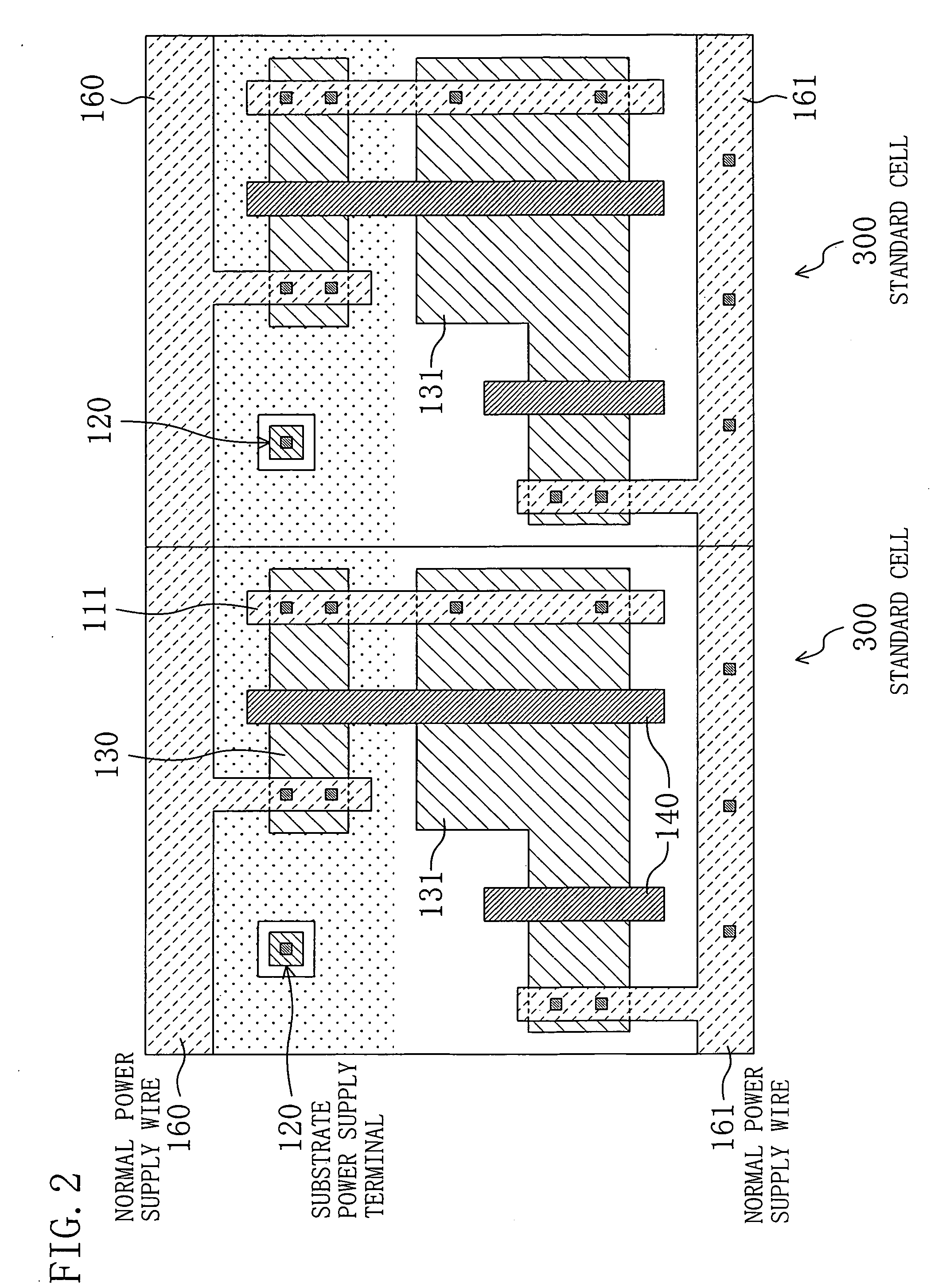
[0081]FIG. 1A illustrates an exemplary standard cell of the present invention. In FIG. 1A, the standard cell 300 is divided into two upper and lower portions, i.e., an n-well region 195 and a p-well region 196. Diffusion layers 130 and 131 are provided in the n-well region 195 and the p-well region 196, respectively. A polysilicon wire 140 is provided on each of the diffusion layers 130 and 131. Also, the polysilicon wire 140 functions as the gates of transistors on each of the diffusion layers 130 and 131. The diffusion layers 130 and 131 are connected through via holes 190 to a metal wire 111. The standard cell 300 also comprises normal power supply wires 160 and 161, and a substrate power supply terminal 120.

[0082] The normal power supply wires 160 and 161 are each a metal wire and are each disposed, extending laterally from a left side to a right side. From the normal power s...

second example

[0097]FIG. 4 illustrates a semiconductor integrated circuit according to a second example of the present invention.

[0098] In FIG. 4, the semiconductor integrated circuit 2999 includes a plurality of standard cell rows 2100 (only seven rows are illustrated in FIG. 4), each of which includes a plurality of standard cells 2000A, 2000B, 2000C, . . . disposed in the same direction (the width direction in FIG. 4). The standard cells 2000A, 2000B, 2000C, . . . have different internal structures, but as illustrated in FIG. 1A, have a common structure in that the normal power supply wires 160 and 161 have the same height position and the same wiring width among the standard cells, and extend in the width direction and disposed into a left side and a right side, and on the other hand, the substrate power supply terminals 120 and 121 are not necessarily formed at the same height position among the standard cells, and are isolated inside not to be disposed into the left side or the right side....

third example

[0123]FIG. 7 illustrates a semiconductor integrated circuit according to a third example of the present invention. Note that, in FIG. 7, the same parts as those of FIG. 4 are indicated by the same reference numerals.

[0124] The semiconductor integrated circuit 3999 of FIG. 7 is different from the semiconductor integrated circuit of FIG. 4 in that inter-cell substrate power supply wires 2013 connect between substrate power supply terminals 2002 of only a portion of a plurality of standard cells 2000. A p-well region and an n-well region of a standard cell 2000 in the semiconductor integrated circuit 3999 of FIG. 7 are shared by standard cells right and left adjacent thereto, respectively, and the substrate potential is the same among the standard cells 2000.

[0125] The semiconductor integrated circuit thus constructed will be hereinafter described.

[0126] The inter-cell substrate power supply wire 2013 of the semiconductor integrated circuit 3999 of FIG. 7 is connected to the substra...


PUM


Abstract

In a standard cell in which a substrate voltage control technique is implemented, a plurality of normal power supply wires are disposed at previously set positions. Therefore, when the standard cell is disposed adjacent to another standard cell having such normal power supply wires, these normal power supply wires are connected to each other. In addition, the standard cell is provided with a substrate power supply terminal which is not connected to that of the other standard cell when the other standard cell is disposed adjacent to the standard cell. Therefore, when a semiconductor integrated circuit is composed of a plurality of the standard cells, a wiring route of an inter-cell substrate power supply wire, or the like can be freely set.

Description

CROSS REFERENCE TO RELATED APPLICATIONS [0001] This Non-provisional application claims priority under 35 U.S.C.§119(a) on Patent Application No. 2005-290397 filed in Japan on Oct. 3, 2005, the entire contents of which are hereby incorporated by reference. BACKGROUND OF THE INVENTION [0002] 1. Field of the Invention [0003] The present invention relates to a standard cell, which is an elementary unit for use in designing layouts of semiconductor integrated circuits, a semiconductor integrated circuit including the standard cells, a method for designing the semiconductor integrated circuit, an apparatus for designing the semiconductor integrated circuit, and a standard cell library. More particularly, the present invention relates to a standard cell which has a substrate control function of controlling a substrate voltage and source voltages of transistors separately, a semiconductor integrated circuit including the standard cells, a method for designing the semiconductor integrated ci...

Claims


Application Information

Patent Timeline
Patent Type & Authority Applications(United States)
IPC IPC(8): H01L27/10H01L29/73
CPCH01L27/0207H01L27/11807
Inventor SHIMBO, HIROYUKIYANO, JUNICHI
Owner PANASONIC CORP
Why Eureka
Try Eureka