

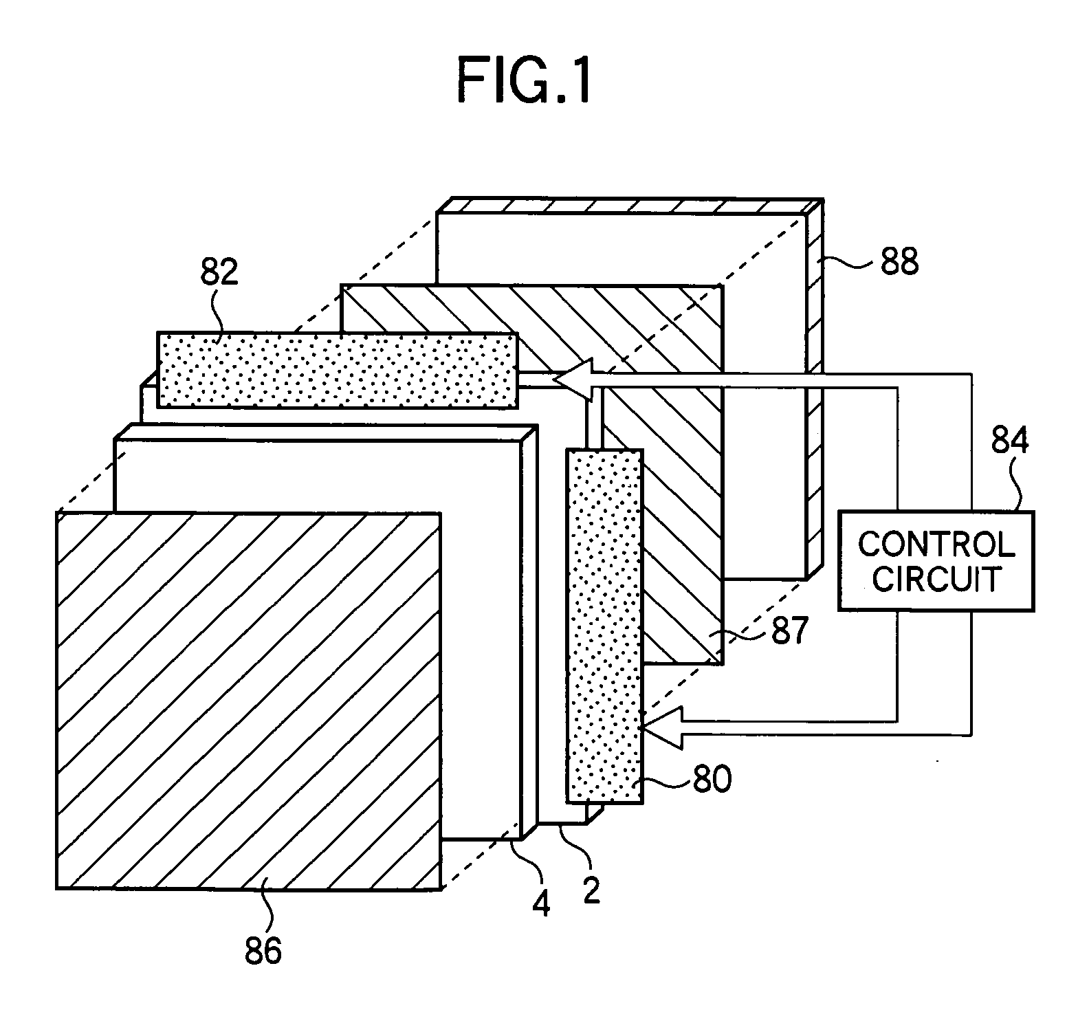
Liquid crystal display device
a liquid crystal display and display device technology, applied in non-linear optics, instruments, optics, etc., can solve the problems of reduced aperture ratio of a pixel, long response time of liquid crystals, and inability to achieve high light transmittance, etc., and achieve excellent display quality
- Summary
- Abstract
- Description
- Claims
- Application Information
AI Technical Summary
Benefits of technology
Problems solved by technology
Method used
Image

Examples
experimental example
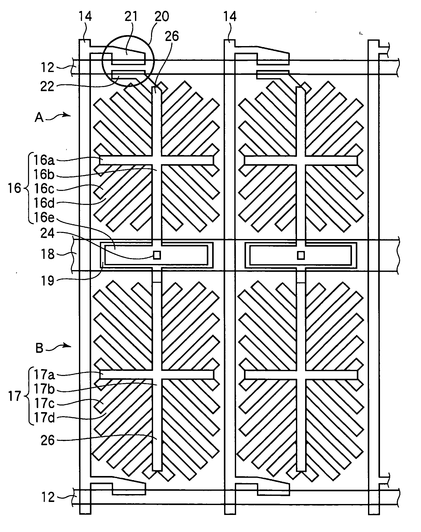
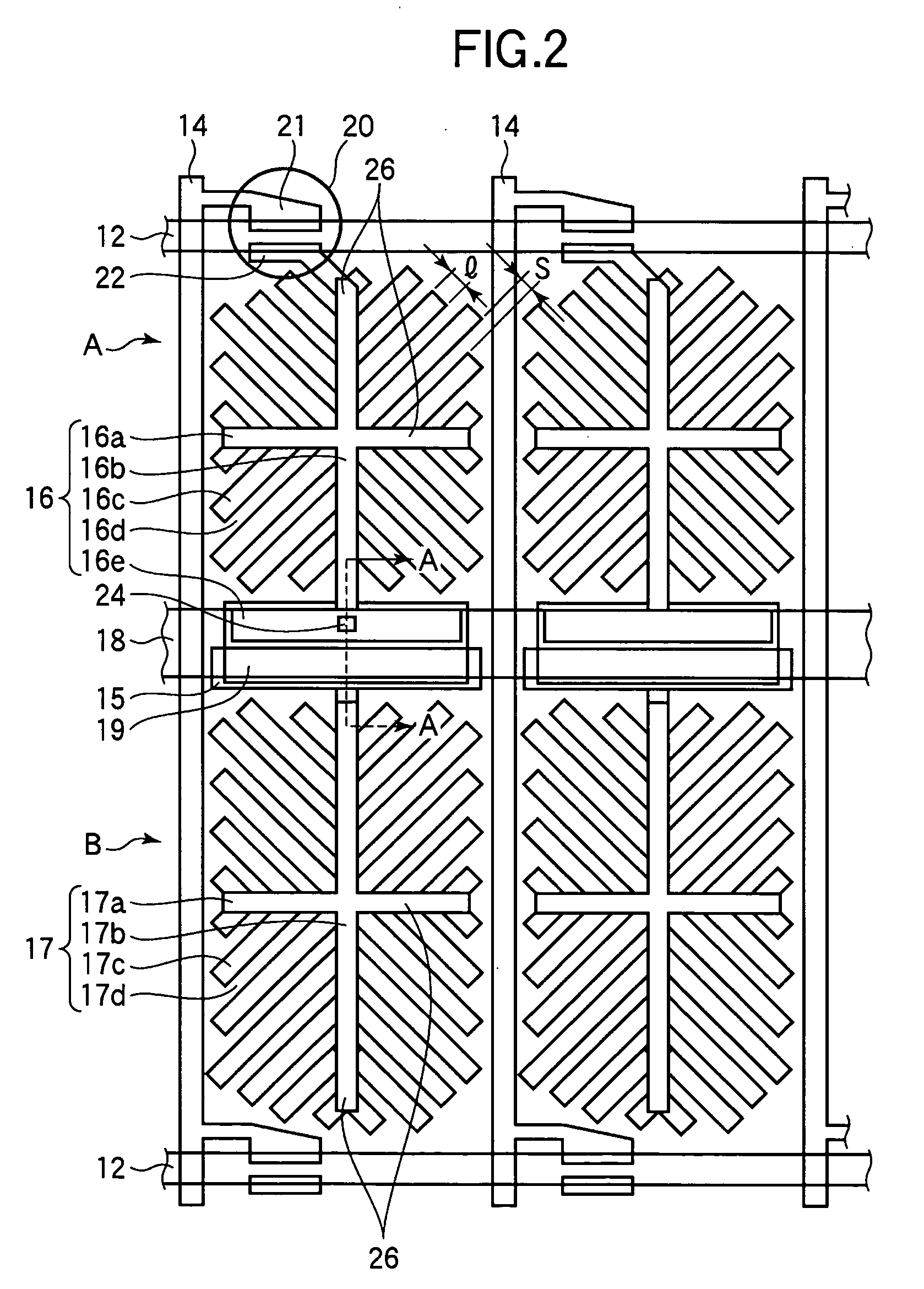
[0051] Six panels were prepared in total: three panels of the liquid crystal display panel using the capacitive coupling HT method in the pixel configuration according to the embodiment shown in FIG. 2, and three conventional panels of a liquid crystal display panel using the capacitive coupling HT method in the pixel configuration in which the dummy capacitive coupling part 15 was not disposed over the storage capacitance bus line 18 and the storage capacitance electrode 19 as shown in FIG. 4 for comparison. For the liquid crystals, liquid crystals of negative dielectric anisotropy containing monomers were used.
[0052] Eight types of AC voltage, 2 V, 2.5 V, 3 V, 5 V, 7.5 V, 10 V, 20 V and 30 V, were applied between the storage capacitance bus line 18 and the common electrode 41 for each of six liquid crystal display panels, and the properties of the alignment of liquid crystals with respect to the applied voltage were tested for the six liquid crystal display panels.
[0053]FIG. 5 i...
PUM
| Property | Measurement | Unit |
|---|---|---|
| width | aaaaa | aaaaa |
| width | aaaaa | aaaaa |
| storage capacitance | aaaaa | aaaaa |
Abstract
Description
Claims
Application Information