System LSI

a technology of system lsi and lsi, applied in the field of system lsi, can solve the problems of unfavorable system lsi area efficiency, and may occur not only with the electric fuse circuit but also with any other circuit, so as to achieve no overhead area and no wasted circuit area

Active Publication Date: 2007-05-03
PANASONIC SEMICON SOLUTIONS CO LTD
View PDF14 Cites 6 Cited by
  • Summary
  • Abstract
  • Description
  • Claims
  • Application Information

AI Technical Summary

Benefits of technology

[0015] In this invention, the I / O power consuming circuit which uses the I / O power source cell as a power source is provided in the layer below the filler cell and is connected to the I / O power source line in the filler cell. As a result, the I / O power consuming circuit is located close to the I / O power source line, so that the line for connecting them is shortened with no wasted circuit area. Hence, an excellent system LSI in which the I / O power source cell is connected to the I / O power consuming circuit at low impedance can be achieved with no area overhead.

Problems solved by technology

This is unfavorable in view of area efficiency of the system LSI.
This problem may occur not only with the electric fuse circuit but also with any other circuits using the I / O power source as a power source.

Method used


Image

  • System LSI
  • System LSI
  • System LSI

Examples


embodiment 1

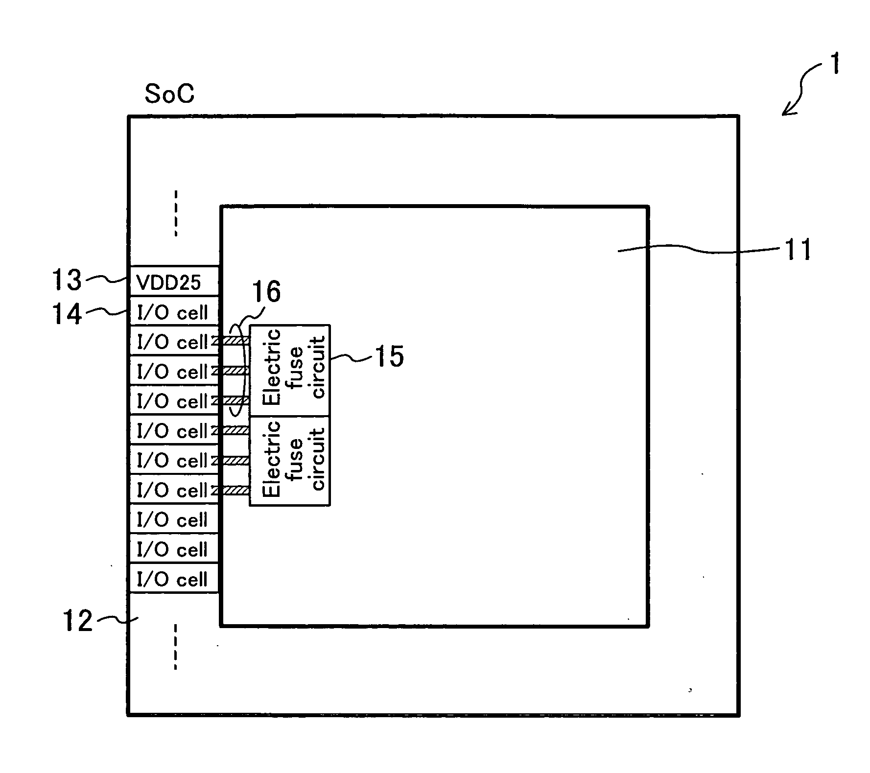
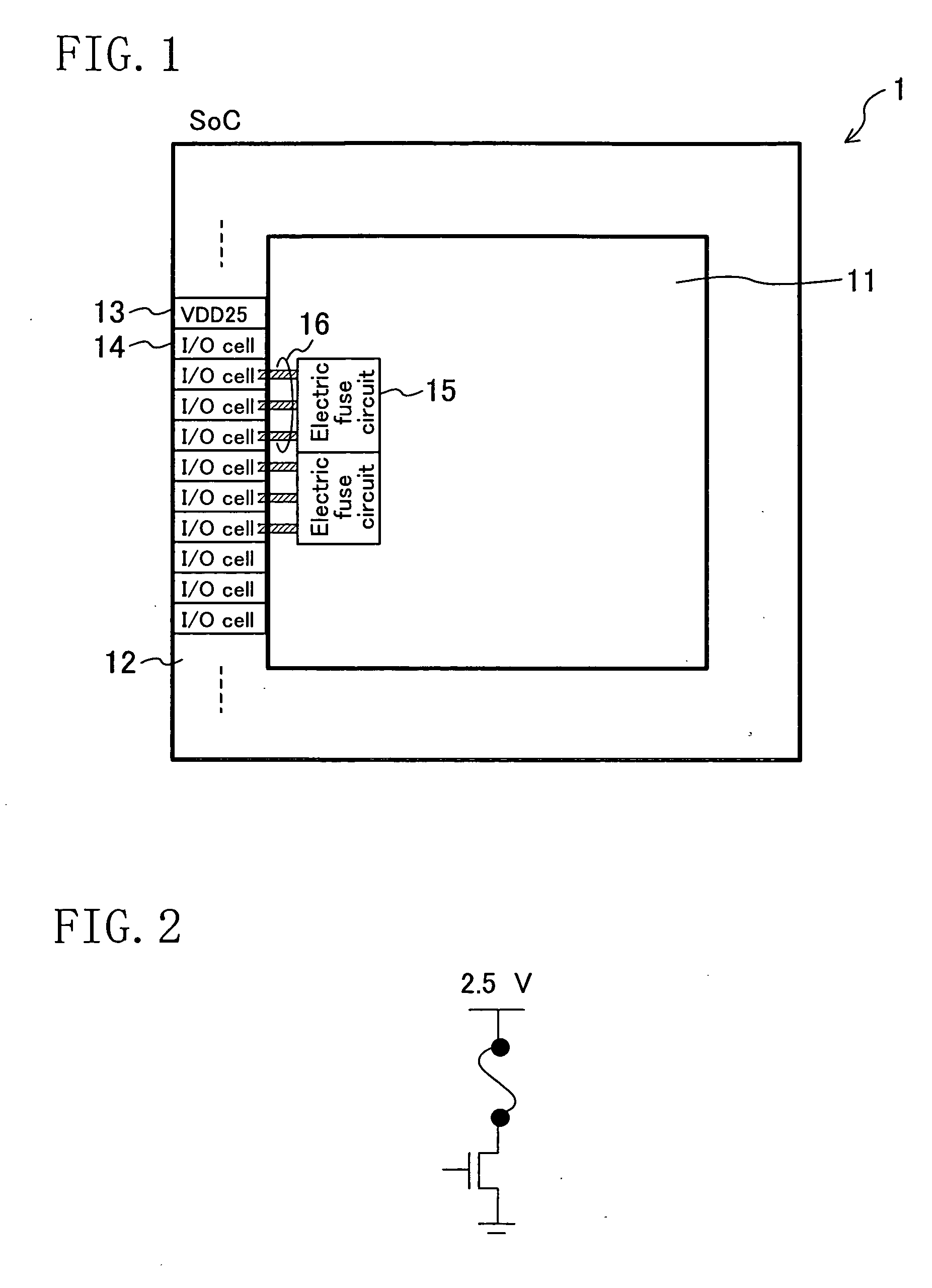
[0025]FIG. 1 is a diagram showing a structure of a system LSI according to Embodiment 1 of the present invention. In FIG. 1, the system LSI (SoC) 1 includes a logic circuit section 11 and an input / output section 12 arranged therearound. The input / output section 12 includes a 2.5V power source cell 13 as an I / O power source cell and a plurality of input / output cells (I / O cells) 14. The logic circuit section 11 includes electric fuse circuits 15 as first I / O power consuming circuits in addition to various logic circuits and RAMs, and the like. The electric fuse circuits 15 use the 2.5 V power source cell 13 as a power source for programming. FIG. 2 is a circuit diagram of an electric fuse circuit. Each electric fuse circuit 15 is connected to a 2.5 V power source line 16 as a first line leading (drawn) from an I / O power source line in at least one (three in FIG. 1) of the I / O cells 14.

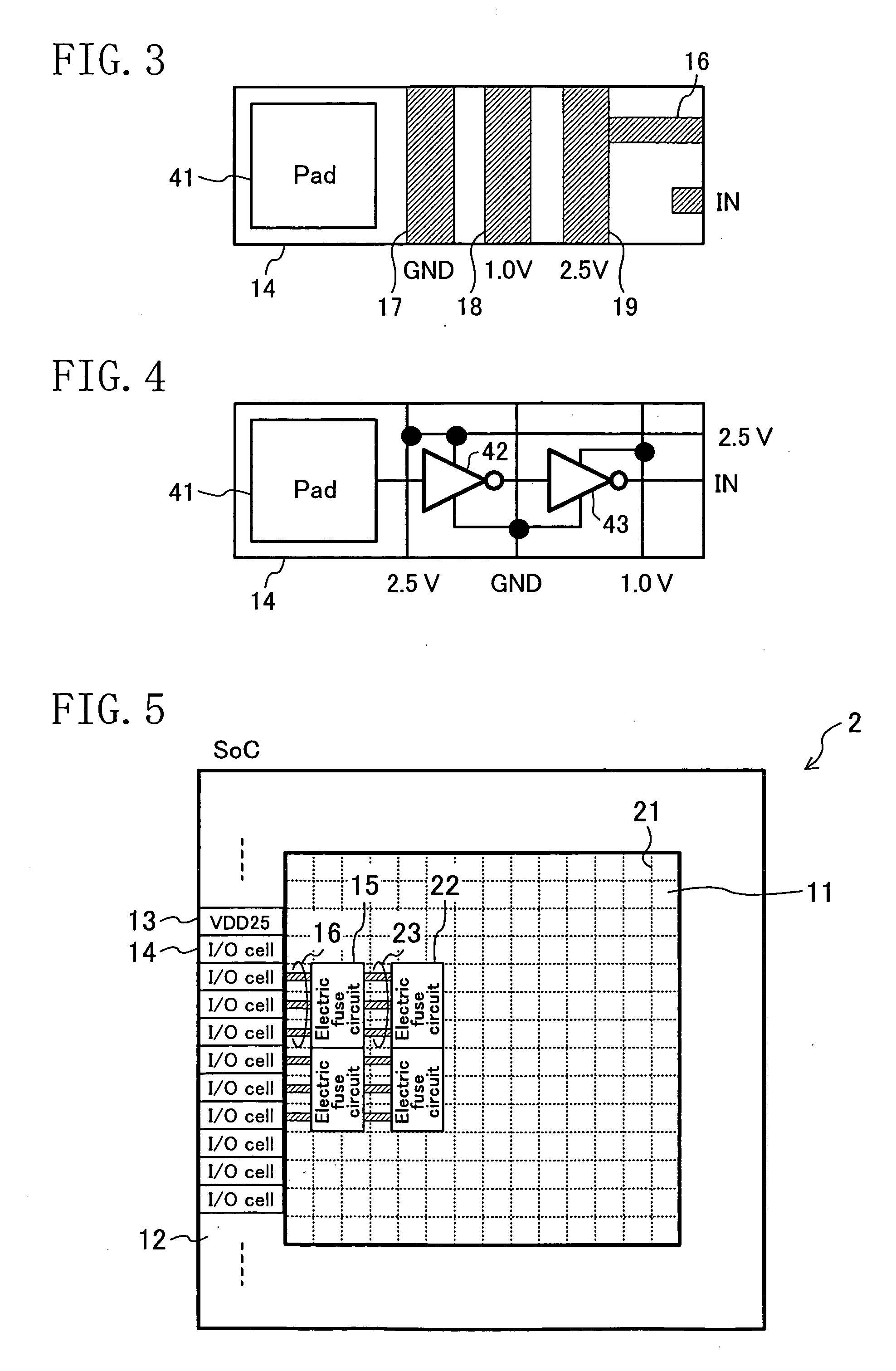
[0026]FIG. 3 and FIG. 4 are a layout diagram and a circuit diagram of an I / O cell 14, respectively, ...

embodiment 2

[0031]FIG. 5 is a diagram showing a structure of a system LSI according to Embodiment 2 of the present invention. In FIG. 5, the same reference numerals are assigned to the constitutional elements common to those in FIG. 1. In the system LSI shown in FIG. 5, a ground line 21 in a mesh-like form is arranged in the logic circuit section 11. Further, electric fuse circuits 22 as second I / O power consuming circuits are provided on the opposite side of the electric fuse circuits 15 from the I / O cells 14. The electric fuse circuits 22 are connected to the electric fuse circuits 15 by means of 2.5 V lines 23 as second lines for supplying electric power from the 2.5 V power source cell 13.

[0032] Power sources and grounds for the logic circuits and the RAMs arranged in the logic circuit section 11 are connected to low-impedance lines usually in mesh-like forms connected to a power source or a ground pad, respectively. For programming an electric fuse circuit, an electric current flowing fro...

embodiment 3

[0036]FIG. 6 and FIG. 7 are diagrams showing I / O cell groups in system LSIs according to Embodiment 3 in the present invention, wherein FIG. 6A and FIG. 7A are layout diagrams, and FIG. 6B and FIG. 7B are sectional views taken along the broken lines X-X′ in FIG. 6A and FIG. 7A, respectively. The same reference numerals are assigned to the constitutional elements common to those in FIG. 3

[0037] In FIG. 6, each I / O cell 14 includes a pad 41 connected to an external terminal and is provided with the ground line 17, the 1.0 V line 18, and the 2.5 V line 19. An electric fuse circuit 31 as an I / O power consuming circuit is provided in a layer below the pads 41. The electric fuse circuit 31 is connected electrically to the 2.5 V line 19 through a wiring layer M4.

[0038] Alternatively, in FIG. 7, a filler cell 32 is provided between a first I / O cell 14a and a second I / O cell 14b. The ground line 17, the 1.0 V line 18, and the 2.5 V line 19 are provided in each of the first and second I / O ce...


PUM


Abstract

A system LSI includes an input/output section and a logic circuit section. The input/output section includes an I/O power source cell having a supply voltage higher than a power source for the logic circuit section and a plurality of I/O cells in each of which an I/O power source line is provided for supplying source power from the I/O power source cell. The logic circuit section includes an I/O power consuming circuit which uses the I/O power source cell as a power source. The I/O power consuming circuit is connected to a line leading from an I/O power source line in at least one of the plurality of I/O cells.

Description

CROSS REFERENCE TO RELATED APPLICATIONS [0001] This Non-provisional application claims priority under 35 U.S.C. § 119(a) on Patent Application No. 2005-300153 filed in Japan on Oct. 14, 2005, the entire contents of which are hereby incorporated by reference. BACKGROUND OF THE INVENTION [0002] 1. Field of the Invention [0003] The present invention relates to a system LSI including a logic circuit section and an input / output section having a plurality of I / O cells, and particularly relates to a system LSI including a circuit which uses an I / O power source as well as the I / O cells. [0004] 2. Background Art [0005] System LSIs in recent years employ a structure in which I / O cells (an input / output section) for input / output are arranged around an LSI and are driven by an I / O power source (at 2.5 V, for example) while logic cells or RAM cells (a logic circuit section) which operate at low voltages are arranged within a range surrounded by the I / O cell group and are driven by a CORE power so...

Claims


Application Information

Patent Timeline
Patent Type & Authority Applications(United States)
IPC IPC(8): H02H3/20
CPCG11C5/063G11C5/14G11C17/165G11C17/18H01L2924/0002H01L2924/00
Inventor AGATA, YASUHIROKAWASAKI, TOSHIAKISHIRAHAMA, MASANORINISHIHARA, RYUJISUMI, SHINICHIYAMAMOTO, YASUEKIKUKAWA, HIROHITO
Owner PANASONIC SEMICON SOLUTIONS CO LTD
Why Eureka
Try Eureka