Capacitor structure

a capacitor and integrated circuit technology, applied in the direction of semiconductor devices, semiconductor/solid-state device details, electrical apparatus, etc., can solve the problems of difficult control of uniformity and stability of insulators, reduced capacitor capacitance, and inability to meet requirements, so as to achieve the effect of not worsening capacitance matching and yield, and greatly increasing unit-area capacitan

Inactive Publication Date: 2007-05-10
UNITED MICROELECTRONICS CORP
View PDF4 Cites 47 Cited by
  • Summary
  • Abstract
  • Description
  • Claims
  • Application Information

AI Technical Summary

Benefits of technology

[0016] Since the capacitor structure of this invention includes two or all of three types of capacitors including MIM, MOM and MIS capacitors and the two or three capacitors are coupled in parallel, the unit-area capacitance is greatly increased. Moreo

Problems solved by technology

When the semiconductor process advances into deep sub-micron generations, the capacitance of capacitor is so reduced that some requirements may not be satisfied.
The first one is to decrease the thickness of the capacitor insulator, but the uniformity and stability of the insulator are difficult to control in this way.
The second one is to increase the surface ar

Method used


Image

  • Capacitor structure
  • Capacitor structure
  • Capacitor structure

Examples


Embodiment Construction

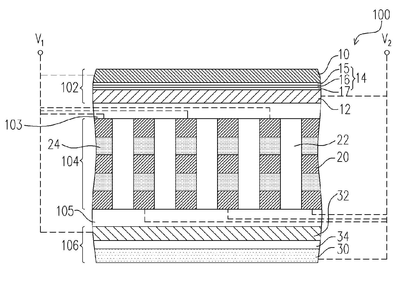
[0021] Referring to FIG. 1, the capacitor structure 100 includes a MIM capacitor 102, a MOM capacitor 104 and a MIS capacitor 106, which three are coupled in parallel. The MIM capacitor 102 includes a first electrode 10, a second electrode 12 under the first electrode 10 and an insulating layer 14 between the two electrodes 10 and 12, wherein the first or second electrode 10 or 12 may be formed from a metal or any other suitable conductive material. The insulating layer 14 may be a composite dielectric layer, such as an ONO layer consisting of a top SiO layer 15, a SiN layer 16 and a bottom SiO layer 17. In other embodiments, the insulating layer 14 can be a single SiO layer.

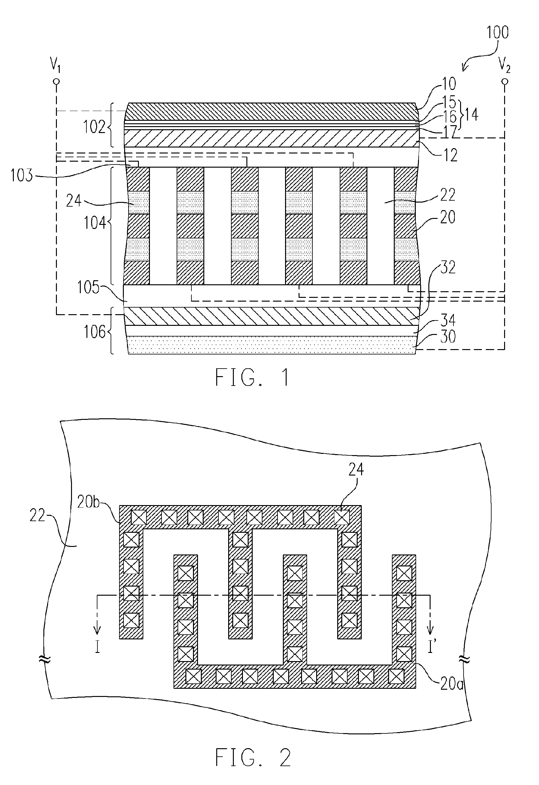
[0022] Referring to FIGS. 1 and 2, the MOM capacitor 104 is disposed under the MIM capacitor 102, including an insulating layer 22, and multiple patterned metal layers 20 and via plugs 24 that constitute a third electrode and a fourth electrode. The patterned metal layers 20 are stacked in the insulating layer ...


PUM


Abstract

A capacitor structure is described, including a first capacitor and a second capacitor. The first capacitor includes a first electrode, a second electrode and a first insulating layer, wherein the second electrode is disposed under the first electrode and the first insulating layer between the first electrode and the second electrode. The second capacitor is disposed under the first capacitor and coupled thereto in parallel. The second capacitor includes multiple patterned metal layers and via plugs that constitute a third electrode and a fourth electrode, and a second insulating layer. The patterned metal layers are stacked in the second insulating layer and connected by the via plugs, wherein each patterned metal layer includes a portion of the third electrode and a portion of the fourth electrode that are separated by the second insulating layer.

Description

BACKGROUND OF THE INVENTION [0001] 1. Field of the Invention [0002] The present invention relates to an IC device structure. More particularly, the present invention relates to a capacitor structure in an integrated circuit. [0003] 2. Description of the Related Art [0004] With the increase in integration degree of integrated circuit, the dimensions of IC devices including capacitors are reduced, so is the capacitance of capacitor. When the semiconductor process advances into deep sub-micron generations, the capacitance of capacitor is so reduced that some requirements may not be satisfied. [0005] There are three ways to increase the capacitance of capacitor in IC design. The first one is to decrease the thickness of the capacitor insulator, but the uniformity and stability of the insulator are difficult to control in this way. The second one is to increase the surface area of the electrodes, but the corresponding fabricating process is quite complicated in this way decreasing the th...

Claims


Application Information

Patent Timeline
IPC IPC(8): H01L27/108H01L29/94H01L29/76H01L31/119
CPCH01L23/5223H01L27/0805H01L2924/0002H01L2924/00
Inventor HSU, TSUN-LAIYEN, ALBERT KUO HUEICHEN, WEI-LIANG
Owner UNITED MICROELECTRONICS CORP
Why Eureka
Try Eureka