

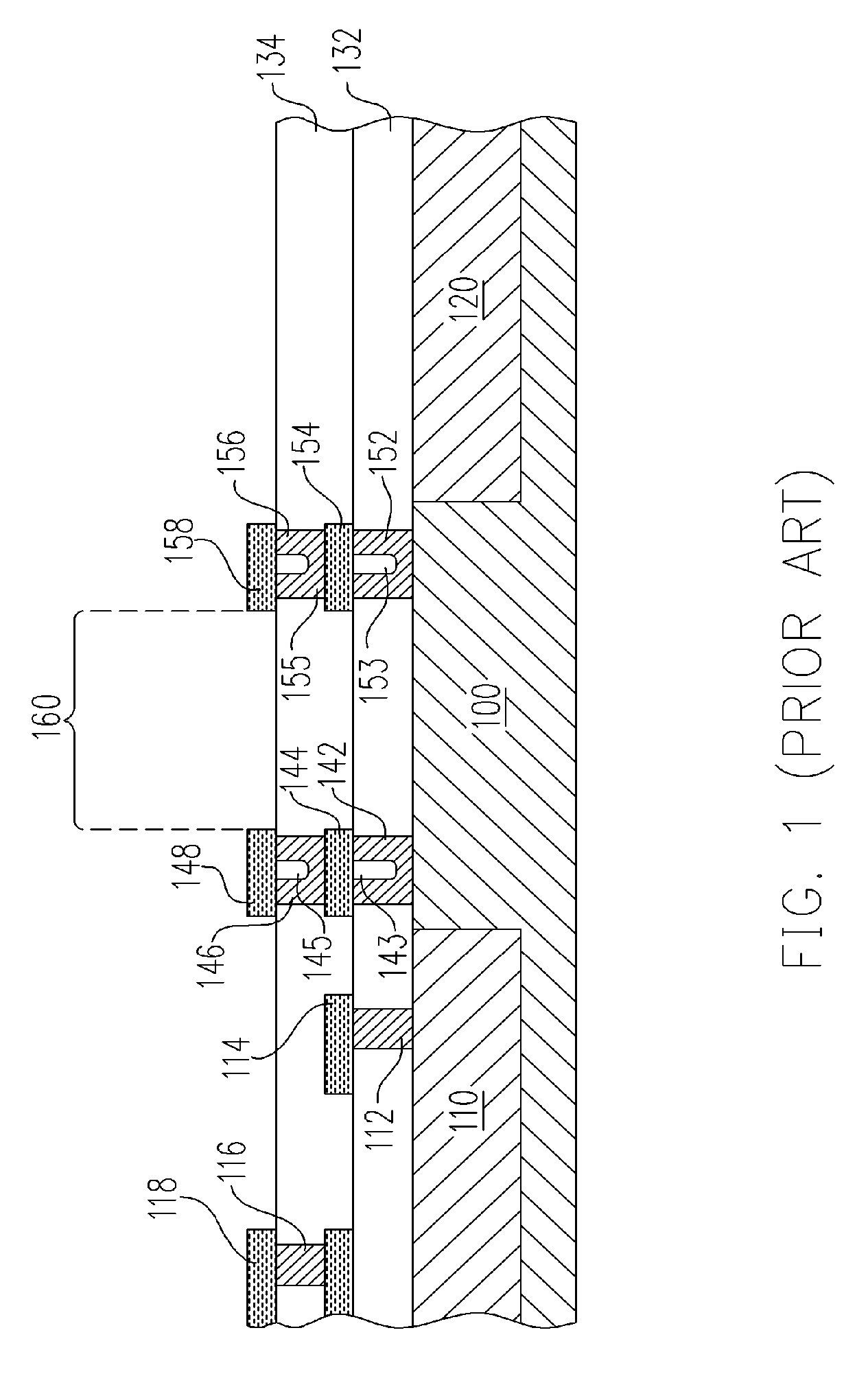
Multi-layer crack stop structure
- Summary
- Abstract
- Description
- Claims
- Application Information
AI Technical Summary
Benefits of technology
Problems solved by technology
Method used
Image

Examples
first embodiment
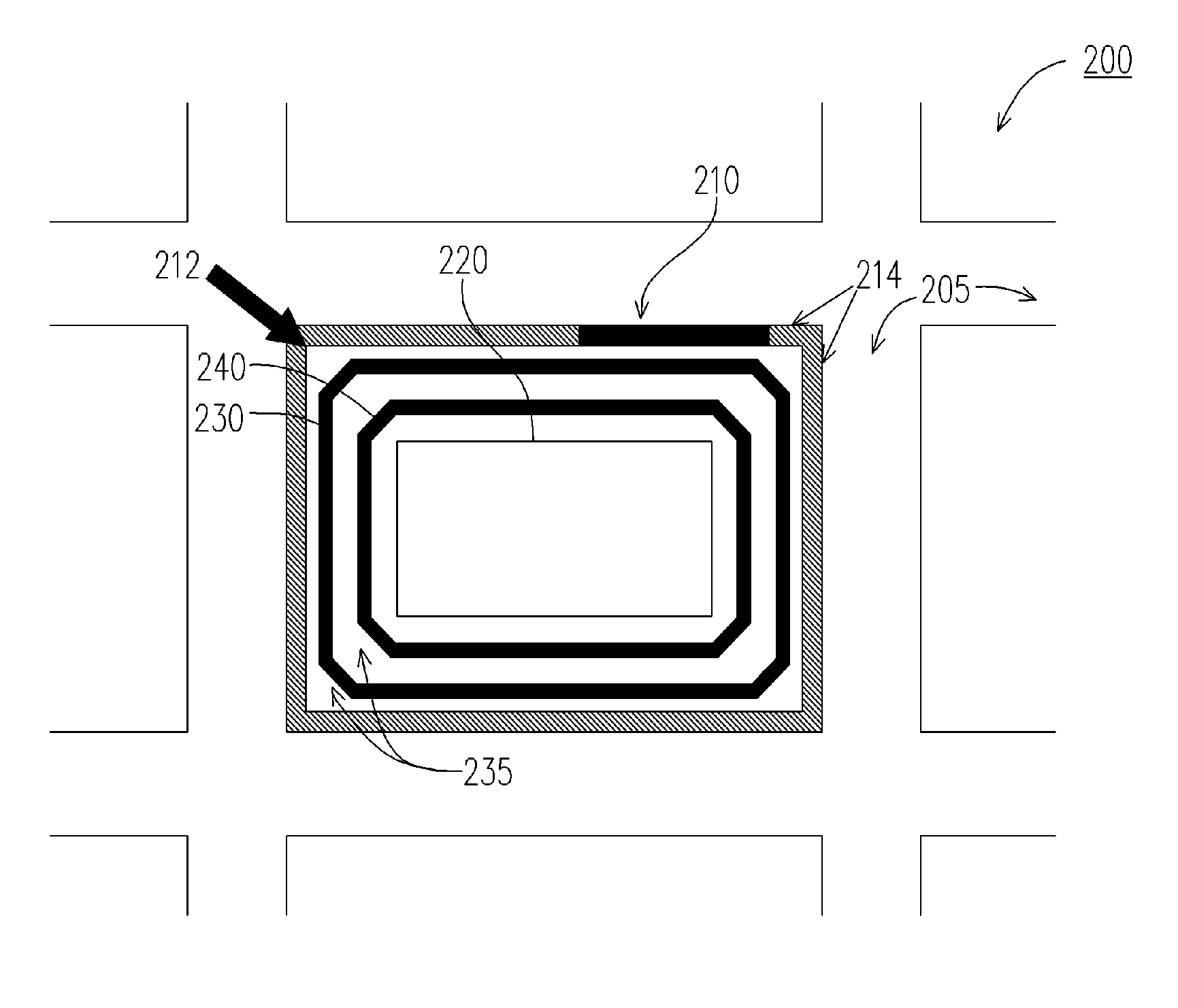
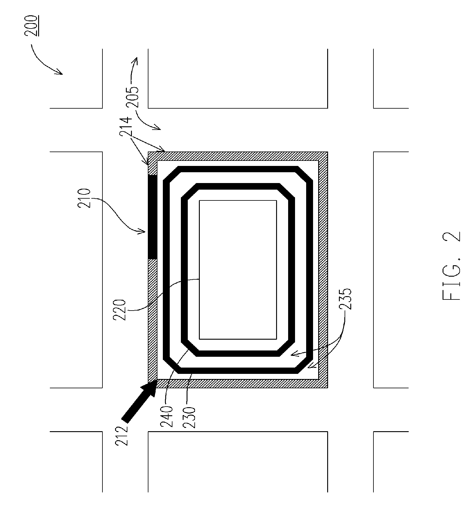
[0034]FIG. 3 illustrates a cross section of a die seal ring structure and an interleaved and staggered multi-layer crack stop structure in this invention. The region 310 for forming the crack stop structure is between the die seal ring region 320 and the scribe line region 305, but may be set at another position in alternative embodiments. The interleaved and staggered multi-layer crack stop structure is formed by interleavedly stacking multiple layers of hollow crack stop units in each of two or more linear regions and staggering the crack stop units in all linear regions in a cross section of the crack stop structure at the same time when the die seal ring is formed in the die seal ring region 320. Therefore, the crack stop units in multiple layers may have the same material. The die seal ring is formed at the same time when the metal layers M1-M9 and the via plugs VIA1-VIA8 between each two layers are formed in the die seal ring region 320, and is connected to the substrate 330 v...
second embodiment
[0037]FIG. 4 illustrates a cross section of a die seal ring structure and a contiguously stacked multi-layer crack stop structure in this invention. The region 410 for forming the crack stop structure is between the die seal ring region 420 and the scribe line region 405, but may be set at another location in alternative embodiments. The multi-layer crack stop structure is formed by contiguously stacking multiple layers of hollow crack stop units 412 at the same time when the die seal ring is formed in the region 420, so that the crack stop units 412 in multiple layers may have the same material.
[0038] The die seal ring is formed at the same time when the multiple metal layers and via plugs between each two layers are interleavedly formed in the die seal ring region 420, and is connected to the substrate 430 via a contact 431 at its bottom. Then, an Al layer 450 and a passivation layer 460 are sequentially formed on the resulting structure. On the other hand, any two adjacent crack ...
third embodiment
[0039]FIG. 5A illustrates a top view of an interleaved and staggered multi-layer crack stop structure according to this invention, and FIG. 5B illustrates a cross section of the same along line V-V′.
[0040] Referring to FIGS. 5A-5B, the interleaved and staggered multi-layer crack stop structure 510 includes multiple separate linear stacks 511 of crack stop units, rather than multiple connected linear stacks as shown in FIG. 3. Each linear stack 511 includes an interleaved stack of hollow crack stop units 512 in multiple dielectric layers 520, wherein each crack stop unit 512 has a void 514 therein. As shown in FIG. 5B, the crack stop units 512 in one linear stack 511 may be interleavedly stacked such that every two adjacent dielectric layers 520 has one crack stop unit 512 therein and the crack stop unit 512 is disposed through the upper one of the two adjacent dielectric layers 520 and into but not through the lower one.
[0041] Meanwhile, the crack stop units 512 in the multiple lin...
PUM
 Abstract
Description
Claims
Application Information