Array substrate for liquid crystal display device and method of fabricating the same
- Summary
- Abstract
- Description
- Claims
- Application Information
AI Technical Summary
Benefits of technology
Problems solved by technology
Method used
Image

Examples
Embodiment Construction
[0045] Reference will now be made in detail to the preferred embodiments of the present invention, examples of which are illustrated in the accompanying drawings.
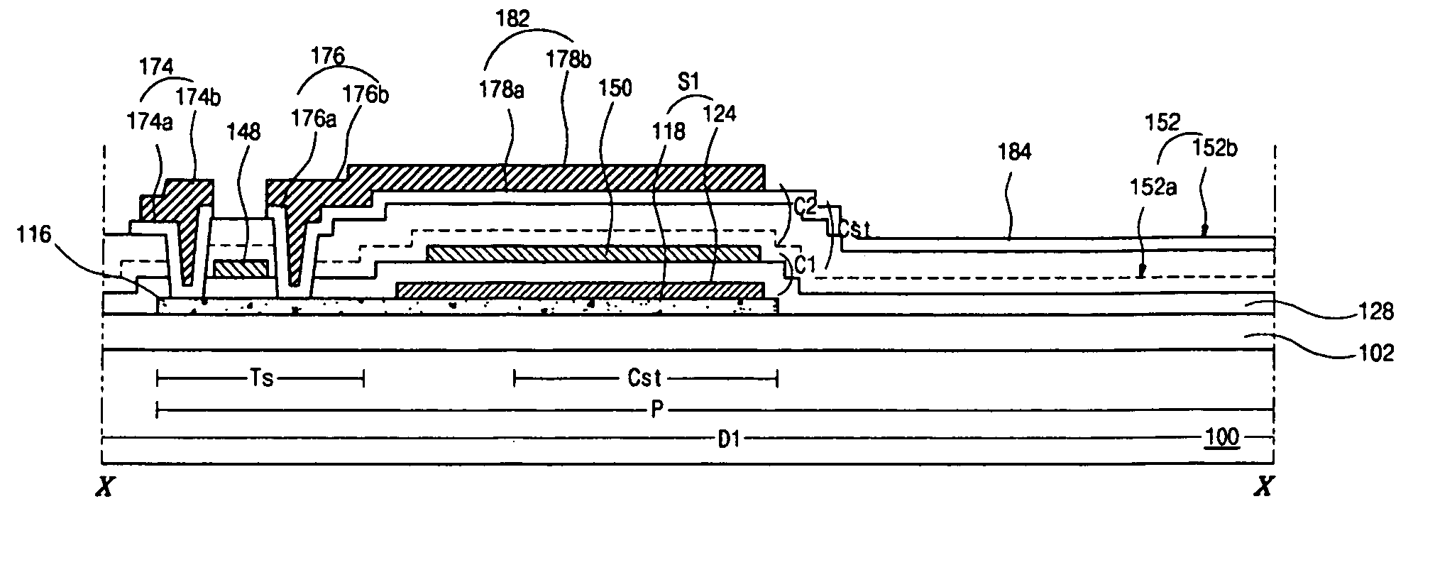
[0046]FIG. 8 is a schematic plane view showing a display region of an LCD device having an integrated driving circuit on the first substrate according to an exemplary embodiment of the present invention. As shown in FIG. 8, gate lines GL and data lines DL are formed on a first substrate 100 and cross each other to define pixel regions P. A switching TFT Ts of polycrystalline silicon is formed at a crossing portion of the gate and data lines GL and DL and includes an active layer 116 of polycrystalline silicon, a gate electrode 148 and a source electrode 174 and a drain electrode 176. A pixel electrode 184 is formed in the pixel region P and contacts the drain electrode 176 of the switching TFT Ts.
[0047] A storage capacitor Cst including a first storage electrode S1, a second storage electrode 150, and a third storage elec...
PUM
 Abstract
Description
Claims
Application Information
 - Generate Ideas
- Intellectual Property
- Life Sciences
- Materials
- Tech Scout
- Unparalleled Data Quality
- Higher Quality Content
- 60% Fewer Hallucinations
Browse by: Latest US Patents, China's latest patents, Technical Efficacy Thesaurus, Application Domain, Technology Topic, Popular Technical Reports.
© 2025 PatSnap. All rights reserved.Legal|Privacy policy|Modern Slavery Act Transparency Statement|Sitemap|About US| Contact US: help@patsnap.com