
Eureka
For R&D, Eureka makes reading and utilizing patents & technical documents easy.
Eureka AIR
Designed for self-driven R&D workflows. Generate viable solutions, solve complex R&D challenges, empower your innovation with AI.

Eureka Materials
Designed for material experts only. Revolutionize your material R&D, from search, analyze, to developing new materials.

TechResearch
Generate reliable direction feasibility study reports for your R&D in just a few steps.

TechSeek
Discover and master advanced knowledge NOW. Basics, ideas, possibilities, all at once.

TechMind
As an expert in R&D Theories, TechMind can generates customized viable solutions instantly.

TechRisk
Analyze your overall solution with one click, know your potential R&D risks in advance.

TechMonitor
Get weekly tech updates, stay abreast of the latest tech innovations and key insights.
Defect inspection device and substrate manufacturing system using the same
- Summary
- Abstract
- Description
- Claims
- Application Information
AI Technical Summary
Benefits of technology
Problems solved by technology
Method used
Image

Examples
first embodiment
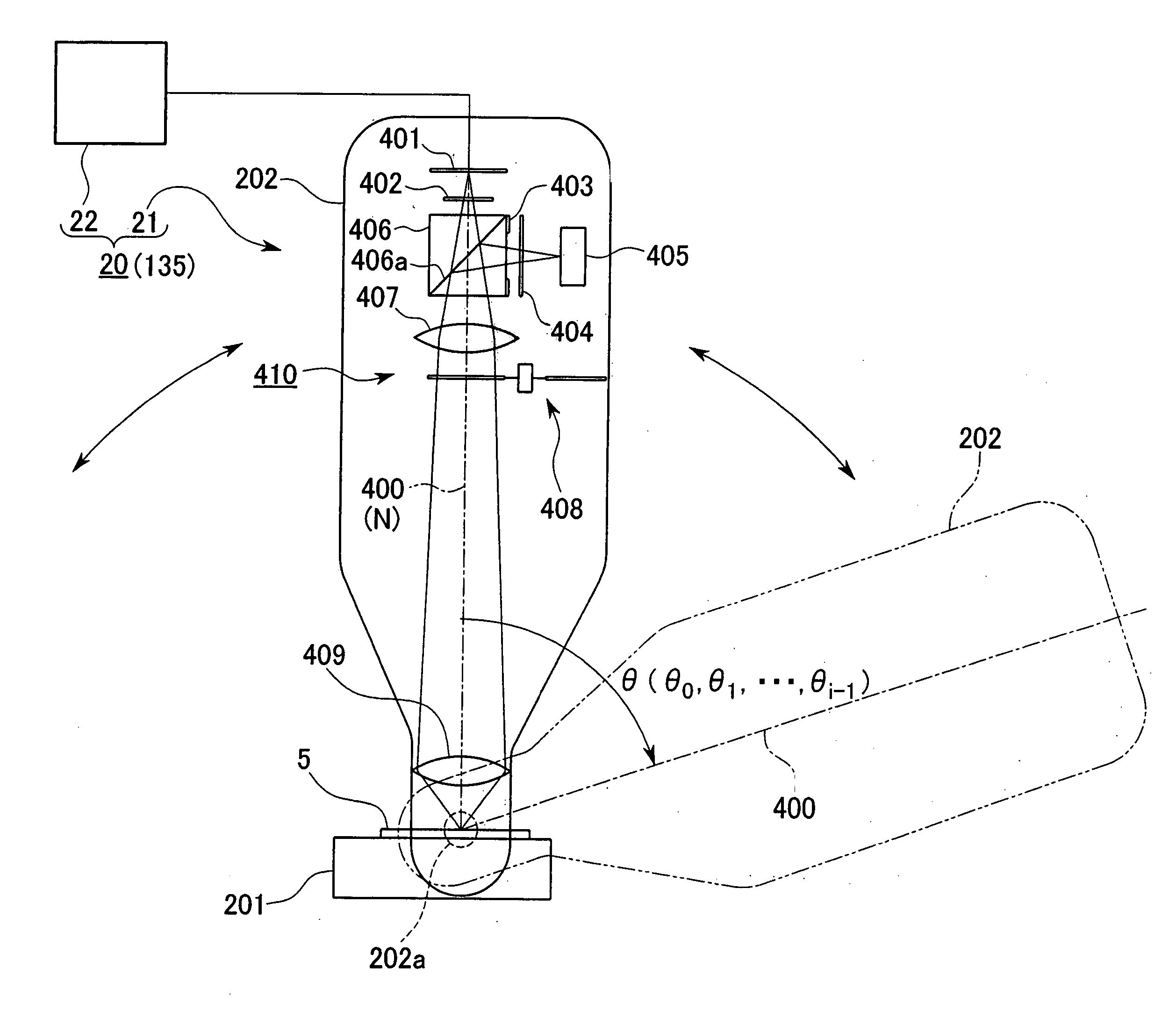
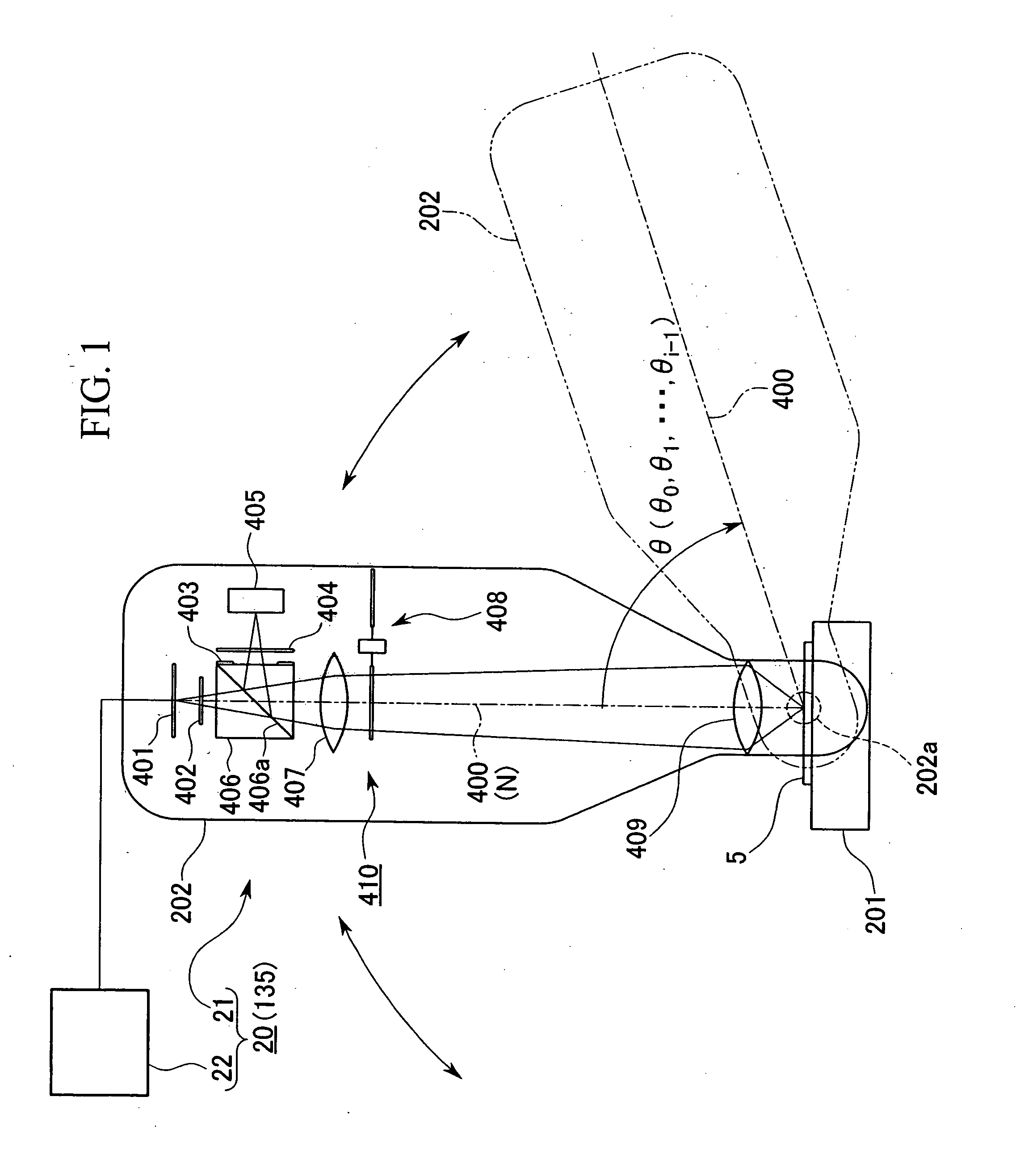
[0023] A defect inspection device according to a first embodiment of the invention will be explained.
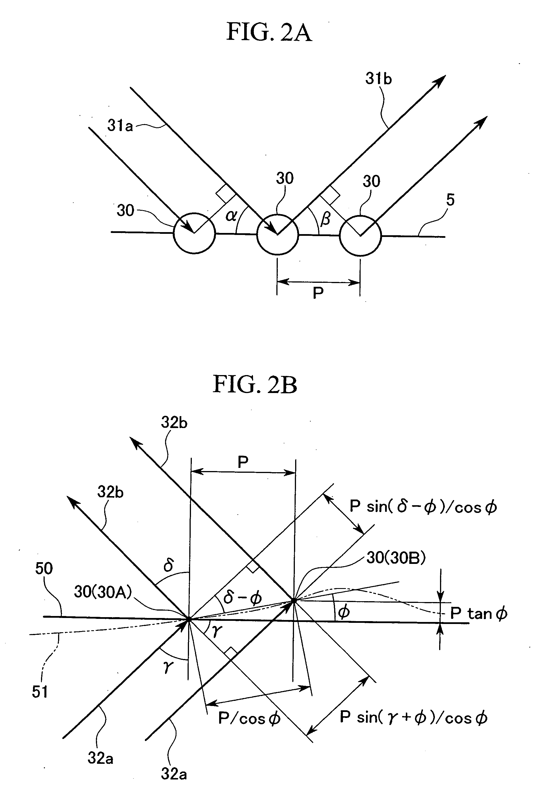
[0024]FIG. 1 is a conceptual diagram for explanation of a schematic configuration of a defect inspection device according to an embodiment of the invention. FIG. 2A is a principle diagram for explanation of light refracted using a regular pattern. FIG. 2B is a schematic optical path diagram representing the relationship between light that is incident on a permeable face and refracted light for explanation of Bragg's law. FIG. 3 is a functional block diagram for explanation of a schematic configuration of a controller / processor of the defect inspection device according to a first embodiment of the invention.
[0025] As shown in FIG. 1, a defect inspection device 20 of this embodiment includes an illumination light-receiving section 21 and a controller / processor 22 that performs various controls and processes images.
[0026] The illumination light-receiving section 21 includes an optica...
second embodiment
[0158] A defect inspection device according to a second embodiment of the invention will be explained.
[0159]FIG. 5 is a conceptual diagram for explanation of a schematic configuration of a defect inspection device according to the second embodiment of the invention. FIG. 6 is a basic explanatory diagram of one example of a plurality of illumination sections used in the defect inspection device according to the second embodiment of the invention. FIG. 7 is a basic explanatory diagram of another example of the same plurality of illumination sections.
[0160] As shown in FIG. 5, a defect inspection device 24 of this embodiment includes an illumination light-receiving section 23 instead of the illumination light-receiving section 21 of the illumination light-receiving section 21 of the first embodiment. The illumination light-receiving section 23 includes an illumination light-receiving section 21, and illumination sections 101 and 102 (at least one of a plurality of illumination sectio...
third embodiment
[0192] A defect inspection device according to a third embodiment of the invention will be explained.
[0193]FIG. 10 is a conceptual diagram for explanation of a schematic configuration of a defect inspection device according to a third embodiment of the invention.
[0194] As shown in FIG. 10, the defect inspection device 28 of this embodiment includes an illumination light-receiving section 27 instead of the illumination light-receiving section 21 of the defect inspection device 20 of the first embodiment. The illumination light-receiving section 27 includes an illumination / light-receiving optical system 430 instead of the illumination / light-receiving optical system 410 of the first embodiment.
[0195] The following explanation centers on points of difference with the first embodiment.
[0196] The illumination / light-receiving optical system 430 includes a light-receiving optical system that excludes the half mirror 406 of the illumination / light-receiving optical system 410 of the first...
PUM
 Abstract
Description
Claims
Application Information
 - R&D Engineer
- R&D Manager
- IP Professional
- Industry Leading Data Capabilities
- Powerful AI technology
- Patent DNA Extraction
Browse by: Latest US Patents, China's latest patents, Technical Efficacy Thesaurus, Application Domain, Technology Topic, Popular Technical Reports.
© 2024 PatSnap. All rights reserved.Legal|Privacy policy|Modern Slavery Act Transparency Statement|Sitemap|About US| Contact US: help@patsnap.com