Method for fabricating high tensile stress film and strained-silicon transistors

a technology of strained silicon and high tensile stress, which is applied in the direction of basic electric elements, electrical equipment, semiconductor devices, etc., can solve the problems of affecting the driving current of the mos transistor, unavoidably limited efficiency, etc., and achieves the effect of increasing the stress of the high tensile stress film

Inactive Publication Date: 2007-05-10
UNITED MICROELECTRONICS CORP
View PDF3 Cites 44 Cited by
  • Summary
  • Abstract
  • Description
  • Claims
  • Application Information

AI Technical Summary

Benefits of technology

[0013] In contrast to the conventional method of fabricating high tensile stress films, the present invention divides the conventional method of just utilizing one deposition process to form a single high tensile stress film and performing one UV curing process on the film into performing multiple deposition processes and multiple heat treatment processes, thereby effectively increasing the stress of the high tensile stress film and the driving current of the NMOS transistor.

Problems solved by technology

However, as the UV curing process often utilizes photons to break the Si—H and SiN—H bond of the silicon nitride to increase stress of the film, the efficiency will be unavoidably limited by the depth of the film.
By performing only a single deposition process to form a layer of high tensile stress film and performing one UV curing process on the high tensile stress film, the efficiency of the UV curing process according to the conventional method of fabricating high tensile stress film will be affected when the depth of the film is overly large, thereby influencing the driving current of the MOS transistors.

Method used


Image

  • Method for fabricating high tensile stress film and strained-silicon transistors
  • Method for fabricating high tensile stress film and strained-silicon transistors
  • Method for fabricating high tensile stress film and strained-silicon transistors

Examples


Embodiment Construction

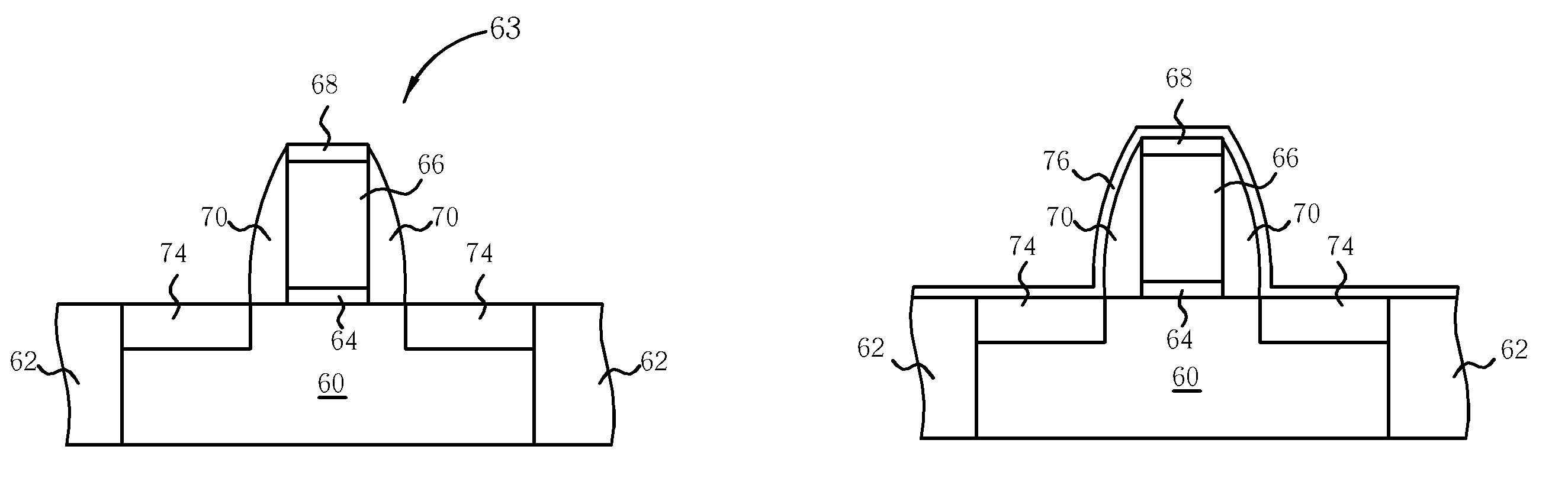
[0017] Please refer to FIG. 4 through FIG. 7. FIG. 4 through FIG. 7 are perspective diagrams showing the means of fabricating a strained-silicon PMOS transistor according to the present invention. As shown in FIG. 4, a semiconductor substrate 60, such as a silicon wafer or a silicon-on-insulator (SOI) substrate, is provided and a gate structure 63 is formed on the semiconductor substrate 60, in which the gate structure 63 includes a gate dielectric 64, a gate 66 disposed on the gate dielectric 64, a cap layer 68 formed on the gate 66, and an ONO offset spacer 70. Preferably, the gate dielectric 64 is composed of silicon dioxide via oxidation or deposition processes, the gate 66 is composed of doped polysilicon, and the cap layer 68 is composed of silicon nitride for protecting the gate 66 or polycide. Additionally, a shallow trench isolation (STI) 62 is formed around the active area of the gate structure 63 within the semiconductor substrate 60.

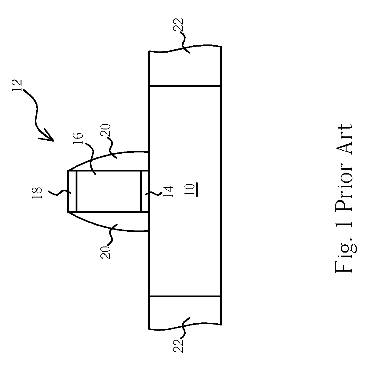
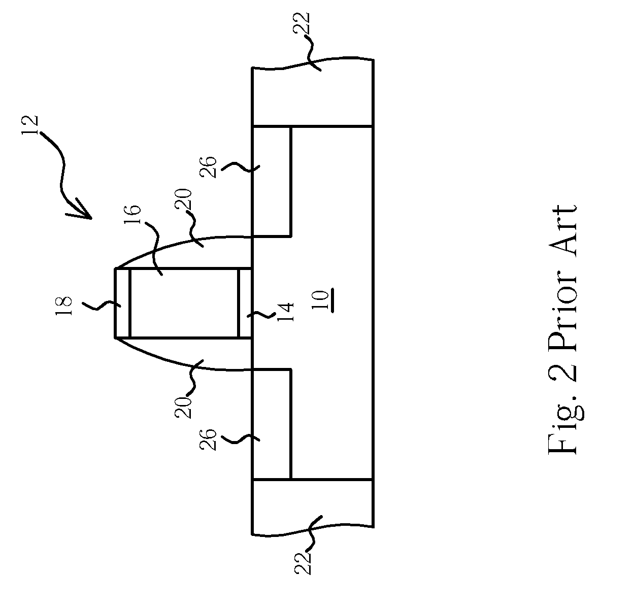
[0018] As shown in FIG. 5, an ion imp...


PUM

PropertyMeasurementUnit
tensile stressaaaaaaaaaa
temperatureaaaaaaaaaa

Abstract

A method for fabricating high tensile stress film and strained-silicon transistors. First, a semiconductor substrate is provided and a gate, at least a spacer, and a source/drain region are formed on the semiconductor substrate. Next, n deposition processes are performed to form n layers of high tensile stress film over the surface of the gate and the source/drain region, in which each high tensile stress film is treated with a heat treatment process and n is greater than or equal to two.

Description

BACKGROUND OF THE INVENTION [0001] 1. Field of the Invention [0002] The invention relates to a method for fabricating high tensile stress film, and more particularly, to a method for forming high tensile stress film on a strained-silicon transistor. [0003] 2. Description of the Prior Art [0004] As semiconductor technology advances and development of integrated circuits revolutionizes, the computing power and storage capacity for computers also increase exponentially, which further increases the expansion of related industries. As predicted by Moore Law, the number of transistors utilized in integrated circuits has been doubled every 18 months and semiconductor processes also have advanced from 0.18 micron in 1999, 0.13 micron in 2001, 90 nanometer (0.09 micron) in 2003, to 65 nanometer (0.065 micron) in 2005. [0005] As the semiconductor processes advance, how to increase the driving current for metal oxide semiconductor (MOS) transistors for fabrication processes under 65 nanometer ...

Claims


Application Information

Patent Timeline
Patent Type & Authority Applications(United States)
IPC IPC(8): H01L21/8234H01L21/336
CPCH01L21/324H01L21/7624H01L29/6656H01L29/78H01L29/7843
Inventor CHEN, NENG-KUOTSAI, TENG-CHUNLIAO, HSIU-LIENHUANG, CHIEN-CHUNG
Owner UNITED MICROELECTRONICS CORP
Why Eureka
Try Eureka