Semiconductor package that includes stacked semiconductor die

a technology of semiconductor dies and semiconductors, applied in the field of new packaging for semiconductor dies, can solve problems such as less than ideal performance, and achieve the effect of saving the area of the board and reducing the consequent parasitics

Inactive Publication Date: 2007-05-17
INFINEON TECH AMERICAS CORP
View PDF3 Cites 35 Cited by
  • Summary
  • Abstract
  • Description
  • Claims
  • Application Information

AI Technical Summary

Benefits of technology

[0004] In a package according to the present invention, two power semiconductor devices are assembled in one package hence saving area on the board and reducing the consequent parasitics.

Problems solved by technology

Furthermore, parasitics due to the extra package elements such as extra lead resistance and inductance result in less than ideal performance.

Method used


Image

  • Semiconductor package that includes stacked semiconductor die
  • Semiconductor package that includes stacked semiconductor die
  • Semiconductor package that includes stacked semiconductor die

Examples


Embodiment Construction

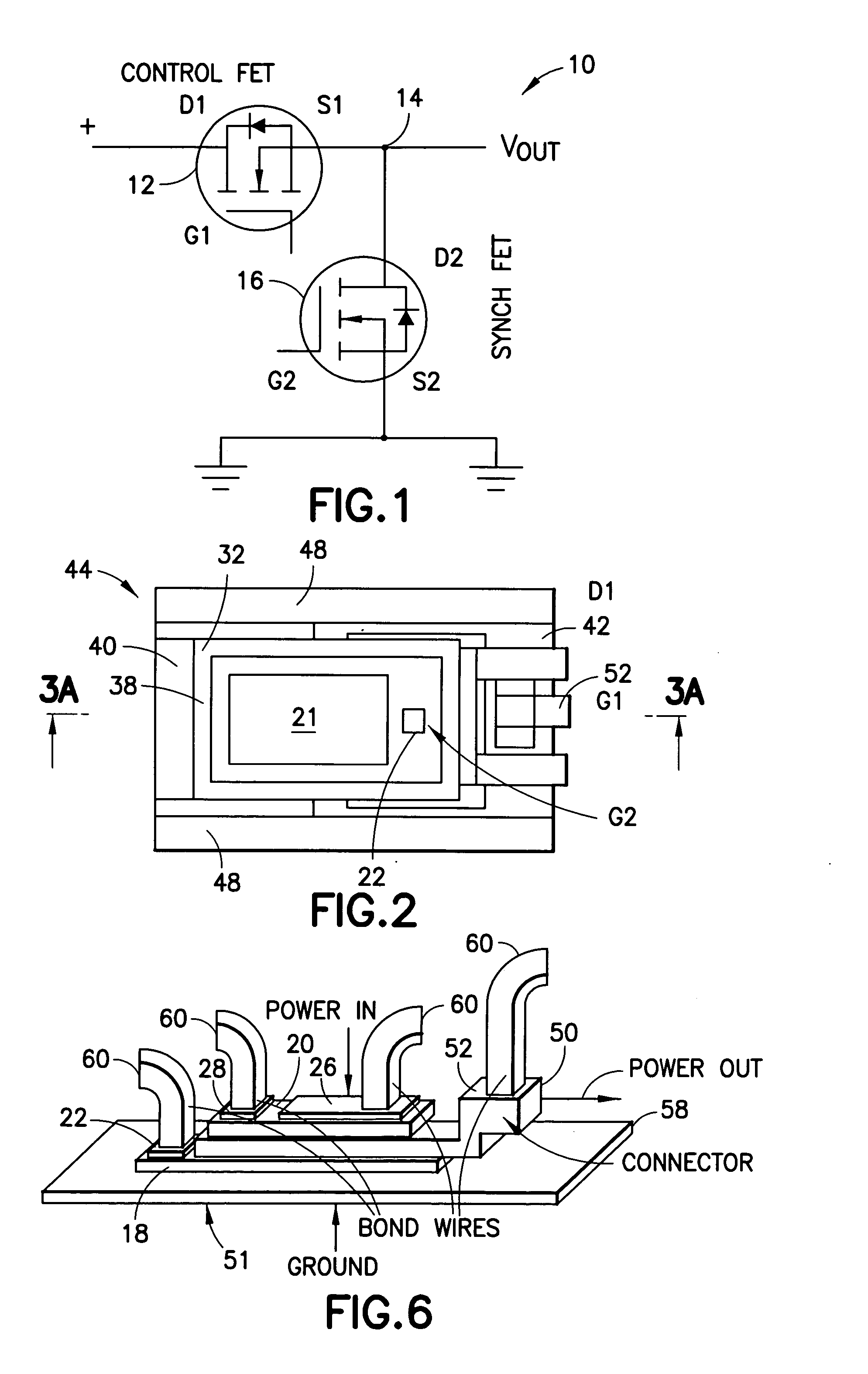
[0015]FIG. 1 shows the switching stage of a DC-DC converter, such as, for example, a buck converter. Switching stage 10 includes a first semiconductor switch 12, e.g., control switch, which may be a power MOSFET, series connected between the voltage input VT and a switched node 14, and a second semiconductor switch 16, e.g., a synchronous switch, which may be a power MOSFET, that is series connected between switched node 14 and the ground. Note that in a typical switching stage 10 first switch 12 may be an N-channel power MOSFET, having its drain electrode D1 connected to the input voltage, and source electrode S1 connected to switched node 14, and second switch 16 may be an N-channel MOSFET having its drain electrode D2 connected to switched node 14 and its source electrode S2 connected to the ground.

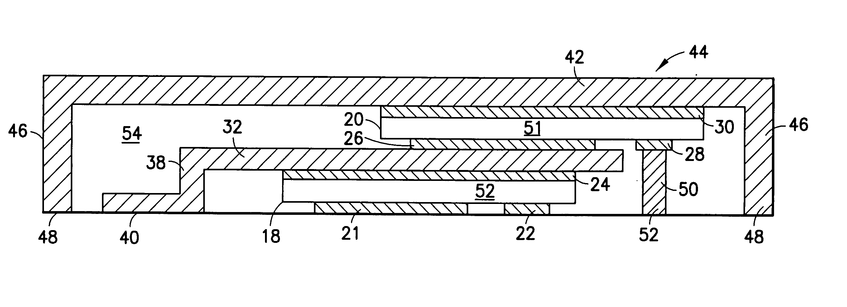
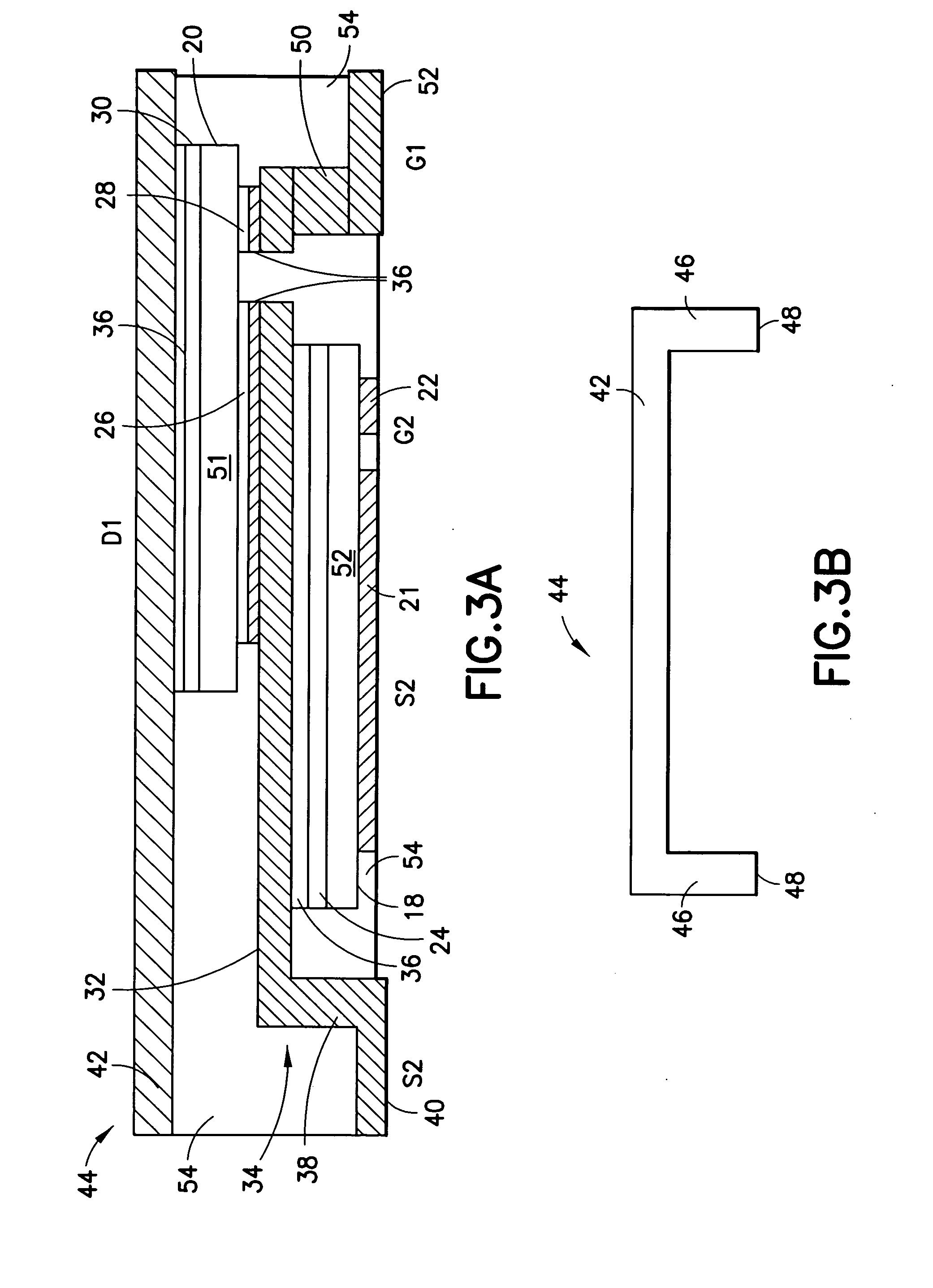
[0016] Referring next to FIGS. 2 and 3A-3B, a semiconductor package according to the first embodiment of the present invention includes a first power switch 18 and a second power swit...


PUM


Abstract

A semiconductor package that includes at least two semiconductor devices that are coupled to one another through a conductive clip.

Description

RELATED APPLICATION [0001] This application is based on and claims benefit of U.S. Provisional Application No. 60 / 733,283, filed on Nov. 3, 2005, entitled Stacked Semiconductor Die For DC / DC Converter with Reduced Foot Print, to which a claim of priority is hereby made and the disclosure of which is incorporated by reference.FIELD OF THE INVENTION [0002] This invention relates to semiconductor devices and more specifically relates to a novel packaging for semiconductor die. BACKGROUND AND SUMMARY OF THE INVENTION [0003] Many power applications require a power stage which usually includes two semiconductor switches that are operatively connected to one another. In many prior art power application applications two individual semiconductor packages are used to obtain the power stage. As a result, the space occupied on the board must accommodate at least two semiconductor packages. Furthermore, parasitics due to the extra package elements such as extra lead resistance and inductance res...

Claims


Application Information

Patent Timeline
Patent Type & Authority Applications(United States)
IPC IPC(8): H01L23/02
CPCH01L23/13H01L23/24H01L2924/00014H01L2224/73253H01L2224/32245H01L2224/293H01L2224/2929H01L2224/85H01L23/3107H01L23/492H01L23/49562H01L23/49575H01L24/40H01L24/83H01L24/85H01L25/074H01L2224/73153H01L2224/83801H01L2224/83851H01L2225/06562H01L2924/01029H01L2924/01082H01L2924/13091H01L2924/16152H01L2924/30107H01L2924/01023H01L2924/01033H01L2924/0665H01L2224/48H01L2924/181H01L2224/84801H01L2224/37147H01L2224/8485H01L2224/37599H01L24/41H01L24/37H01L24/84H01L2924/00012H01L2224/45015H01L2924/207H01L2224/45099
Inventor MONTGOMERY, ROBERT
Owner INFINEON TECH AMERICAS CORP
Why Eureka
Try Eureka