Method of manufacture of silicon based package and devices manufactured thereby

Inactive Publication Date: 2007-05-17
GLOBALFOUNDRIES U S INC
View PDF11 Cites 22 Cited by
  • Summary
  • Abstract
  • Description
  • Claims
  • Application Information

AI Technical Summary

Benefits of technology

[0016] b) forming unique structures comprising metal capture pads or metal capture vias as the first level of metal placed on the silicon surface to prepare for creation of the vias, with the metal capture pads serving as a natural etch stop, allowing creation of the vias without requiring extremely precise etch control or without pre-etching and filling vias by a conventional via filling process;
[0018] d) minimizing the number of through vias required in the combined silicon / carrier structure, which enables the use of large reliable vias to be utilized.
[0020] An advantage of this invention is the ability to support very high wiring density packaging applications with low cost silicon based processing technology.
[0054] Experimentation has shown that when a VSTV design is substituted for a TSTV design, the resulting devices are operable and are less expensive than the TSTV devices because the VSTV devices require only a single masking step on the wafer backside instead of two masking steps, and a VSTV design does not limit the silicon carrier thickness to be >150 microns as had been thought prior the present invention. Furthermore, the present invention eliminates the significant problem of achieving a thin and uniform thickness resist layer which is required for imaging of the second via mask used in the tapered via process.

Problems solved by technology

A problem with using silicon based structures for electronic packaging applications is the need for getting vias through the silicon from the bottom surface through the silicon to the top of the silicon where the wiring structure is fabricated.

Method used


Image

  • Method of manufacture of silicon based package and devices manufactured thereby
  • Method of manufacture of silicon based package and devices manufactured thereby
  • Method of manufacture of silicon based package and devices manufactured thereby

Examples


Embodiment Construction

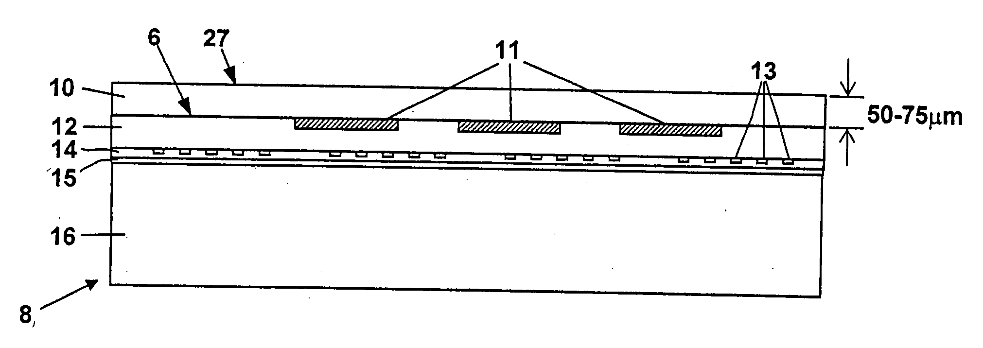
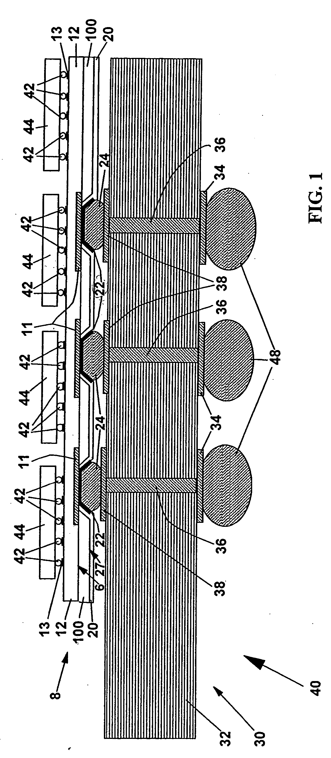
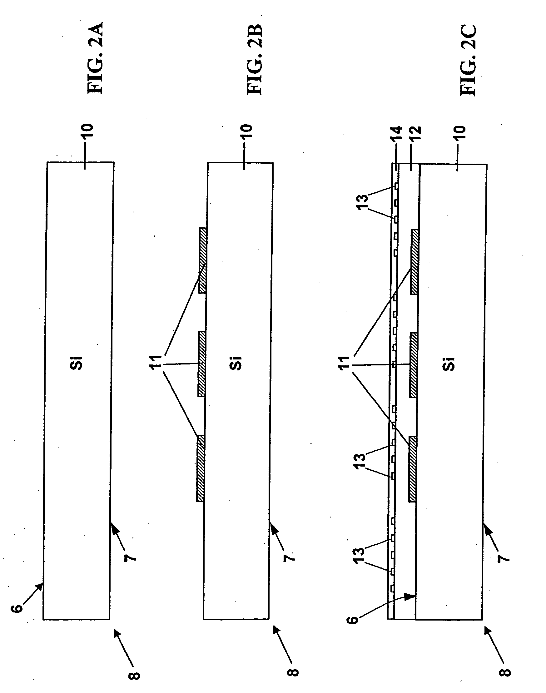
[0061]FIG. 1 is a schematic sectional diagram of an embodiment of a combined package 40 including an Silicon Based Package (SBP) 8 mounted on an MLC (Multi-Layer Ceramic) package carrier 30 in accordance with this invention. FIGS. 2A-2M illustrate the steps of a method in accordance with this invention for forming a package of the kind shown in FIG. 1. Package 8 includes a UTSW 100 with a substantially planar upper surface 6 as well as a substantially planar, thinned reverse surface 27 that is covered, on the lower surface thereof, with a dielectric material 20. An array of BLM metal via pads 22 have been formed extending through openings through the dielectric material 20 and the UTSW 100 to the top surface 6 thereof.

[0062] Micro-BGAs 24 have been formed joined to the array of conductive UTSW BLM metal via pads 22 extending from the top surface 6 through to the thinned reverse surface 27 of the UTSW 100. Above each UTSW BLM metal via 22 is a metal capture pad 11, each of which ser...


PUM


Abstract

A Silicon Based Package (SBP) is formed starting with a thick wafer, which serves as the base for the SBP, composed of silicon which has a first surface and a reverse surface which are planar. Then form an interconnection structure including metal capture structures in contact with the first surface and multilayer conductor patterns over the first surface. Form a temporary bond between the SBP and a wafer holder, with the wafer holder being a rigid structure. Thin the reverse side of the wafer to a desired thickness to form an Ultra Thin Silicon Wafer (UTSW) for the SBP. Form via holes with tapered or vertical sidewalls, which extend through the UTSW to reach the metal capture structures. Then form metal pads in the via holes which extend through the UTSW, making electrical contact to the metal capture structures. Then bond the metal pads in the via holes to pads of a carrier.

Description

BACKGROUND OF THE INVENTION [0001] 1. Field of the Invention [0002] This invention relates to semiconductor devices and more particularly to a method of manufacturing semiconductor packaging. [0003] 2. Description of Related Art [0004] U.S. Pat. No. 5,497,545 of Watanabe et al. for “Method of Making Electrical Connections in the Manufacture of Wiring Sheet Assemblies” describes a multilayer conductor stack formed on a polyimide or ceramic carrier having first and second conductor separated by an insulator sheet are electrically interconnected by a stud inserted through a hole formed in the second conductor and the insulator sheet. Wire bonding and stamping secure the stud to the conductors, thereby forming an electrical connection. [0005] U.S. Pat. No. 5,654,590 of Kuramochi for “Multichip-Module Having an HDI and a Temporary Supporting Substrate” starts with a bonding layer composed of a material such as silicon, aluminum or epoxy resin formed over a temporary supporting base with ...

Claims


Application Information

Patent Timeline
Patent Type & Authority Applications(United States)
IPC IPC(8): H01L21/00H01L21/44H01L21/48H01L21/68
CPCH01L21/486H01L21/6835H01L21/6836H01L21/76898H01L23/147H01L24/16H01L2221/68318H01L2221/68327H01L2221/6834H01L2221/68345H01L2221/68354H01L2221/68363H01L2224/16237H01L2924/01046H01L2924/01078H01L2924/01079H01L2924/14H01L2924/15311H01L2224/16225H01L2924/12042H01L2924/00014H01L2224/05571H01L2924/00H01L2224/0401H01L2924/00012
Inventor MAGERLEIN, JOHN H.PATEL, CHIRAG S.SPROGIS, EDMUND J.STOLLER, HERBERT I.
Owner GLOBALFOUNDRIES U S INC
Why Eureka
Try Eureka