Method of manufacture of silicon based package

a technology of silicon based packaging and manufacturing method, which is applied in the direction of semiconductor devices, semiconductor/solid-state device details, electrical apparatus, etc., to achieve the effect of minimizing the number of through vias and large reliable vias

Inactive Publication Date: 2005-04-12
GLOBALFOUNDRIES INC
View PDF23 Cites 54 Cited by
  • Summary
  • Abstract
  • Description
  • Claims
  • Application Information

AI Technical Summary

Benefits of technology

A problem with using silicon based structures for electronic packaging applications is the need for getting vias through the silicon, i.e. from the bottom surface through the silicon to the top of the silicon where the wiring structure is fabricated. This invention solves the above problem by some or all of the techniques as follows:a) using a wafer thinning process to create a silicon structure thin enough for ‘reasonable sized’ vias to be created;b) forming unique structures comprising capture pads as the first level of metal placed on the silicon surface to prepare for creation of the vias, with the capture pads serving as a natural etch stop, allowing creation of the vias without requiring extremely precise etch control or without pre-etching and filling vias by a conventional via filling process;c) using a sacrificial glass plate as a holder to facilitate handling of ultra thin silicon wafers; and / ord) minimizing the number of through vias required in the combined silicon / carrier structure, which enables the use of large reliable vias to be utilized.

Problems solved by technology

A problem with using silicon based structures for electronic packaging applications is the need for getting vias through the silicon, i.e. from the bottom surface through the silicon to the top of the silicon where the wiring structure is fabricated.

Method used


Image

  • Method of manufacture of silicon based package
  • Method of manufacture of silicon based package
  • Method of manufacture of silicon based package

Examples


Embodiment Construction

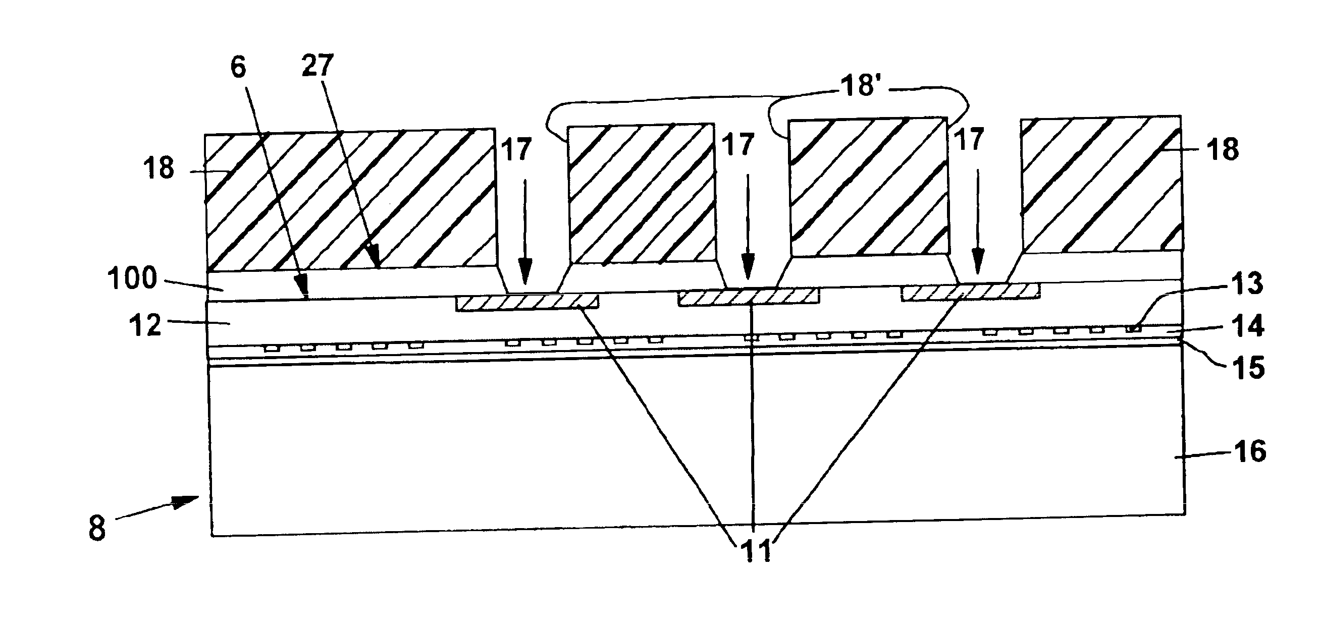
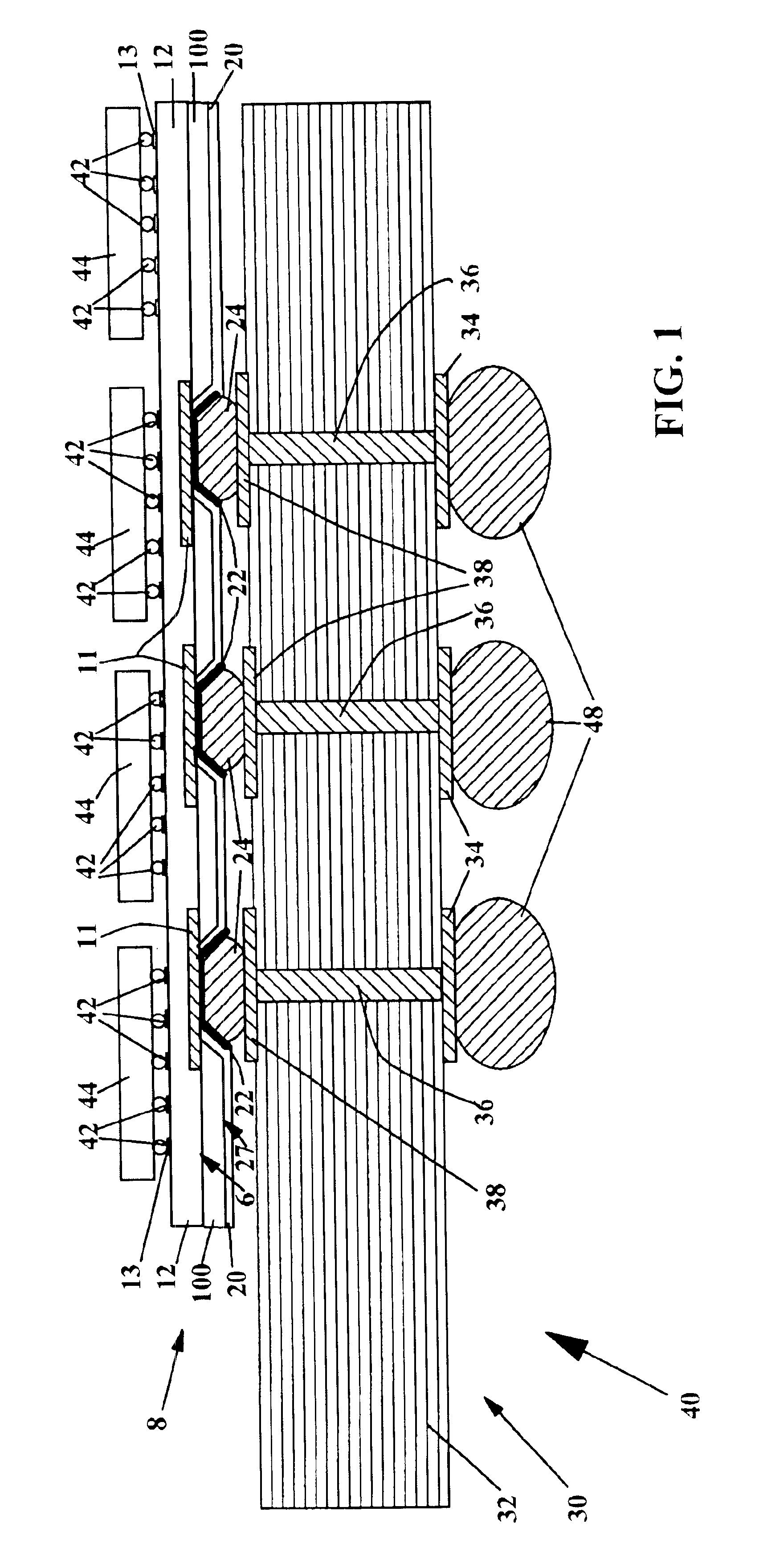
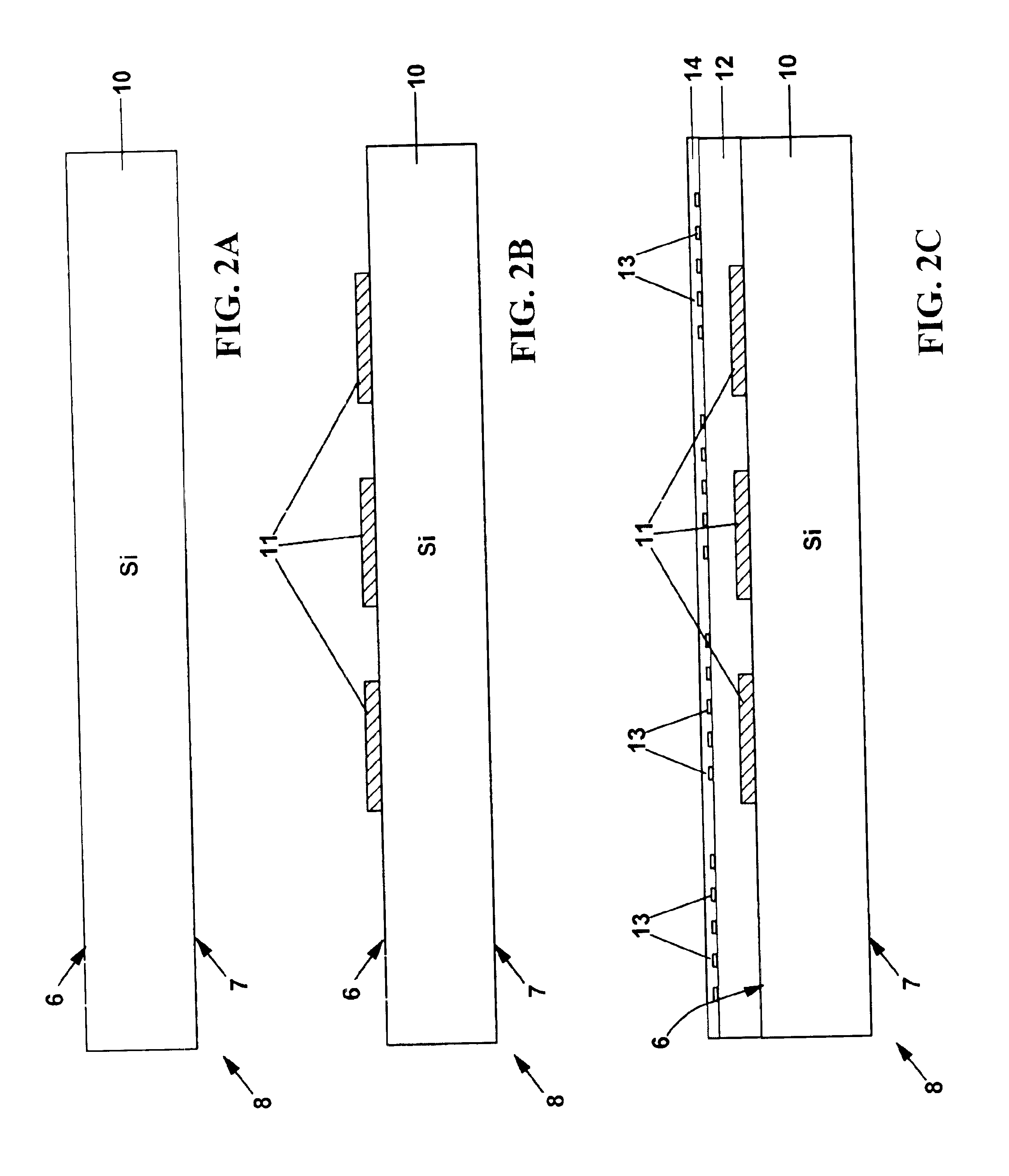
FIG. 1 is a schematic sectional diagram of an embodiment of a combined package 40 including a Silicon Based Package (SBP) 8 mounted on a multilayer ceramic package carrier 30 in accordance with this invention. The steps of a method for forming a package of the kind shown in FIG. 1 are illustrated by FIGS. 2A-2M. Package 8 includes an Ultra-Thin Silicon Wafer (UTSW) 100 with a planar upper surface 6 and a planar lower surface 27 covered, on the lower surface thereof, with a dielectric material 20. An array of vias 22 have been formed extending through openings through the dielectric material 20 and the UTSW 100 to the top surface 6 thereof. Micro-BGAs 24 have been formed joined to the array of conductive UTSW vias 22 extending from the top surface 6 through to the lower surface 27 of the UTSW 100. Above each UTSW via 22 is a metal capture pad 11, each of which served as an etch stop when the holes in which the UTSW vias 22 are located were being formed. The upper surface of the UTSW ...


PUM

PropertyMeasurementUnit
thickaaaaaaaaaa
thicknessaaaaaaaaaa
thicknessaaaaaaaaaa

Abstract

A silicon based package (SBP) is formed starting with a thick wafer, which serves as the base for the SBP, composed of silicon which has a first surface and a reverse surface which are planar. Then form an interconnection structure including multilayer conductor patterns over the first surface. Form a temporary bond between the SBP and a wafer holder, with the wafer holder being a rigid structure. Thin the wafer to a desired thickness to form an Ultra Thin Silicon Wafer (UTSW) for the SBP. Forming via holes which extend through the UTSW, forming metallization in the via holes which extends through the UTSW, making electrical contact to the interconnection structure on the first surface. Then bond the metallization in the via holes to pads of a carrier.

Description

BACKGROUND OF THE INVENTION1. Field of the InventionThis invention relates to semiconductor devices and more particularly to a method of manufacturing semiconductor packaging.2. Description of Related ArtU.S. Pat. No. 5,497,545 of Watanabe et al. for “Method of Making Electrical Connections in the Manufacture of Wiring Sheet Assemblies” describes a multilayer conductor stack formed on a polyimide or ceramic carrier having first and second conductor separated by an insulator sheet are electrically interconnected by a stud inserted through a hole formed in the second conductor and the insulator sheet. Wire bonding and stamping secure the stud to the conductors, thereby forming an electrical connection.U.S. Pat. No. 5,654,590 of Kuramochi for “Multichip-Module Having an HDI and a Temporary Supporting Substrate” starts with a bonding layer composed of a material such as silicon, aluminum or epoxy resin formed over a temporary supporting base with a temporary supporting layer composed of...

Claims


Application Information

Patent Timeline
Patent Type & Authority Patents(United States)
IPC IPC(8): H01L21/68H01L21/02H01L21/48H01L21/67
CPCH01L21/486H01L21/6835H01L24/16H01L2221/6834H01L2221/68345H01L2221/68354H01L2924/15311H01L2224/16237H01L2924/01046H01L2924/01078H01L2924/01079H01L2924/14H01L2221/68363H01L2924/12042H01L2924/00
Inventor BROFMAN, PETER J.DAVES, GLENN G.RAY, SUDIPTA K.STOLLER, HERBERT I.
Owner GLOBALFOUNDRIES INC
Why Eureka
Try Eureka