Method for fabricating dislocation-free stressed thin films

a stress-free, thin film technology, applied in semiconductor/solid-state device manufacturing, basic electric elements, electric apparatus, etc., can solve the problems of reducing and reducing the cost of production, so as to reduce the size of the device and increase the cost of production

Inactive Publication Date: 2007-05-17
RGT UNIV OF CALIFORNIA
View PDF6 Cites 13 Cited by
  • Summary
  • Abstract
  • Description
  • Claims
  • Application Information

AI Technical Summary

Problems solved by technology

Unfortunately, there are several disadvantages to graded silicon germanium buffer layers.
First, the threading dislocation density, while lower in graded buffer layers, is still non-zero, which leads to degradation of electron and hole mobility.
The large thickness increases the size of the devices as well as the cost of production.
Second, the strain-relaxed graded silicon germanium buffer layer has a rough surface which degrades the mobility of strained silicon.
In addition, the strain at the top layer of silicon is not homogeneous due to the stress fields from buried dislocations, which also adversely affects carrier transport.

Method used


Image

  • Method for fabricating dislocation-free stressed thin films
  • Method for fabricating dislocation-free stressed thin films
  • Method for fabricating dislocation-free stressed thin films

Examples


Embodiment Construction

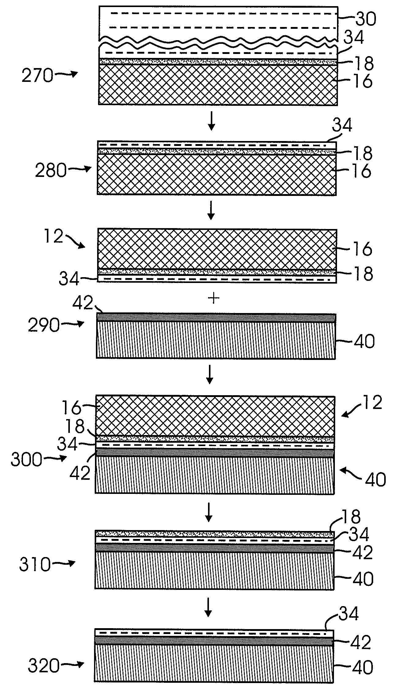
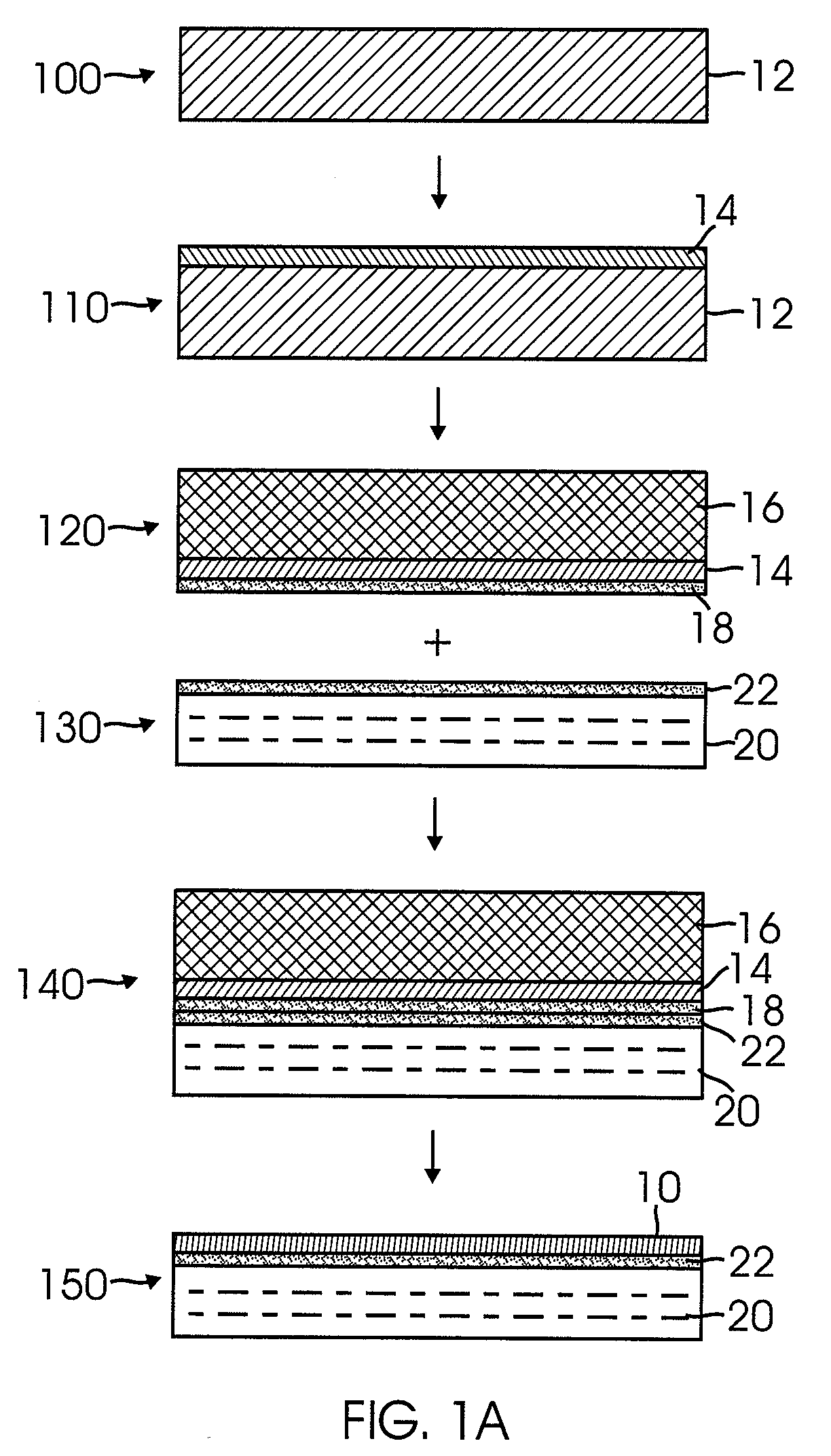
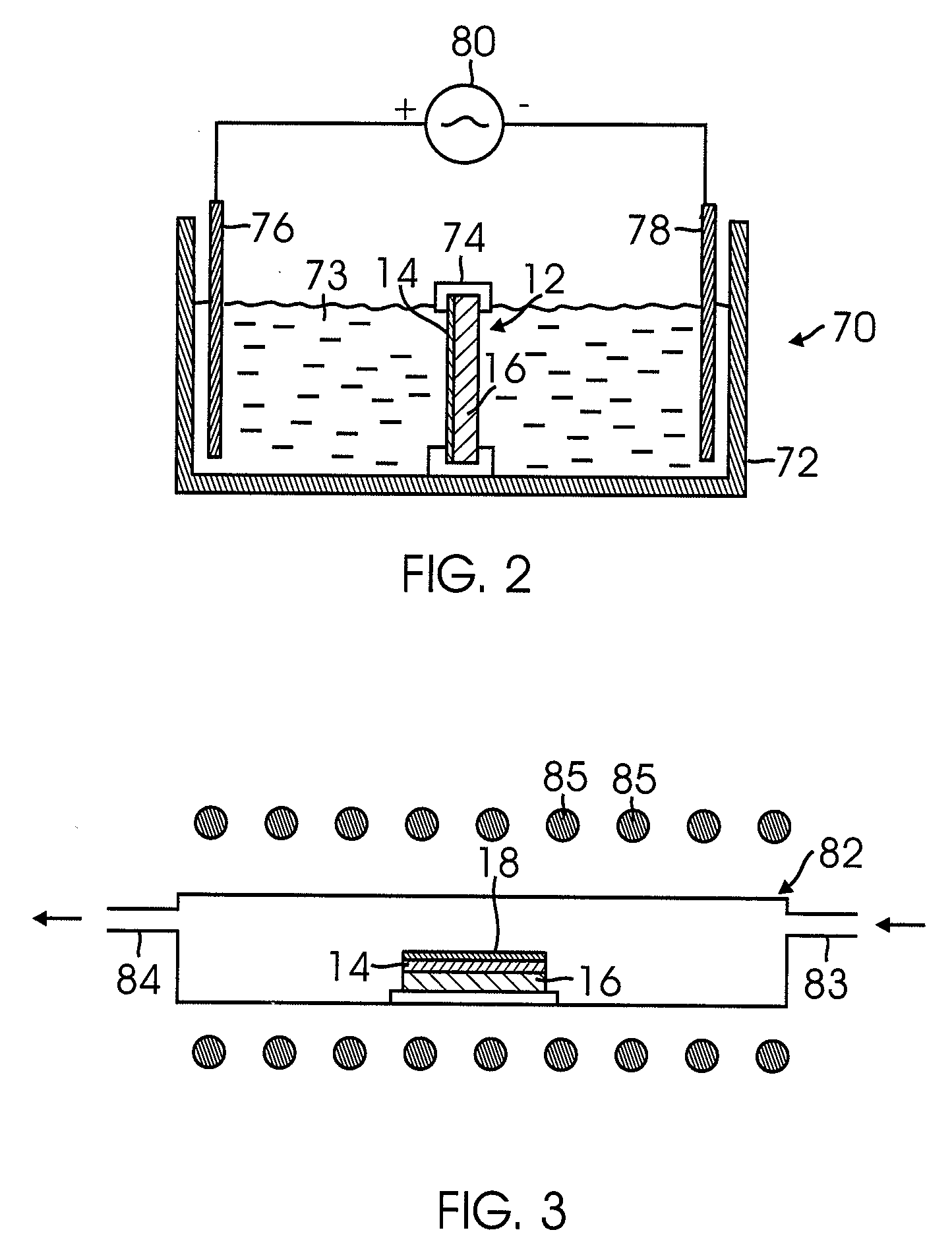
[0016]FIG. 1A illustrates a process of forming a homogeneously stressed thin film 10 on a transfer substrate 20 according to one embodiment of the invention. Initially, in step 100, a first substrate 12 is provided. The first substrate 12 may be formed from a semiconductor material, or in some instances, an insulator material. For example, in one aspect of the embodiment, the substrate 12 is formed from a doped, p+ type silicon substrate. The substrate 12 may be formed as wafer or the like such that the homogeneously stressed thin film 10 (described in more detail below) may be formed across (and subsequently transferred from) substantially the entire surface of the substrate 12. The p+ silicon substrate 12 is heavily doped with a doping agent such as boron, although other doping agents known to those skilled in the art may also be used.

[0017] In step 110, an un-doped epilayer 14 of silicon is formed on the doped, p+ type silicon substrate 12. Alternatively, n-type silicon may be u...


PUM

PropertyMeasurementUnit
thicknessaaaaaaaaaa
temperatureaaaaaaaaaa

Abstract

A method of forming a stressed thin film on a substrate includes the steps of depositing a thin film of silicon on a first substrate and transforming the first substrate into a porous substrate. The porous substrate containing the thin film of silicon is then transformed into a stressed state such that at least a portion of the stress is transferred to the thin film. The thin film may be under compressive stress or tensile stress. For example, volumetric expansion of the porous substrate imparts tensile stress to the thin film while volumetric contraction of the porous substrate imparts compressive stress to the thin film. The porous substrate containing the stressed thin film of silicon is then bonded to a second substrate. The porous substrate is removed so as to deposit the stressed thin film of silicon to the second substrate.

Description

REFERENCE TO RELATED APPLICATIONS [0001] This Application claims priority to U.S. Provisional Patent Application No. 60 / 700,448 filed on Jul. 19, 2005. U.S. Provisional Patent Application No. 60 / 700,448 is incorporated by reference as if set forth fully herein.STATEMENT REGARDING FEDERALLY SPONSORED RESEARCH AND DEVELOPMENT [0002] The U.S. Government may have a paid-up license in this invention and the right in limited circumstances to require the patent owner to license others on reasonable terms as provided for by the terms of contract number: No. FA9550-04-1-0370 awarded by the United States Air Force.FIELD OF THE INVENTION [0003] The field of the invention generally relates to methods for forming stressed (e.g., compressive of tensile) thin films. More particularly, the field of the invention relates to methods used to form dislocation-free stressed thin films. BACKGROUND OF THE INVENTION [0004] The use of strained silicon devices is known to increase semiconductor device perfor...

Claims


Application Information

Patent Timeline
Patent Type & Authority Applications(United States)
IPC IPC(8): H01L21/76
CPCH01L21/76256H01L21/2007
Inventor XIE, YA-HONGKIM, JEEHWAN
Owner RGT UNIV OF CALIFORNIA
Why Eureka
Try Eureka