
Organic light emitting diode display

a light-emitting diode and organic technology, applied in the direction of discharge tube luminescnet screens, discharge tube/lamp details, electric discharge lamps, etc., can solve the problems of liquid crystal display, large volume and weight, and difficulty in portability, so as to minimize interference

Inactive Publication Date: 2007-05-24
SAMSUNG DISPLAY CO LTD
View PDF4 Cites 9 Cited by
  • Summary
  • Abstract
  • Description
  • Claims
  • Application Information

AI Technical Summary

Benefits of technology

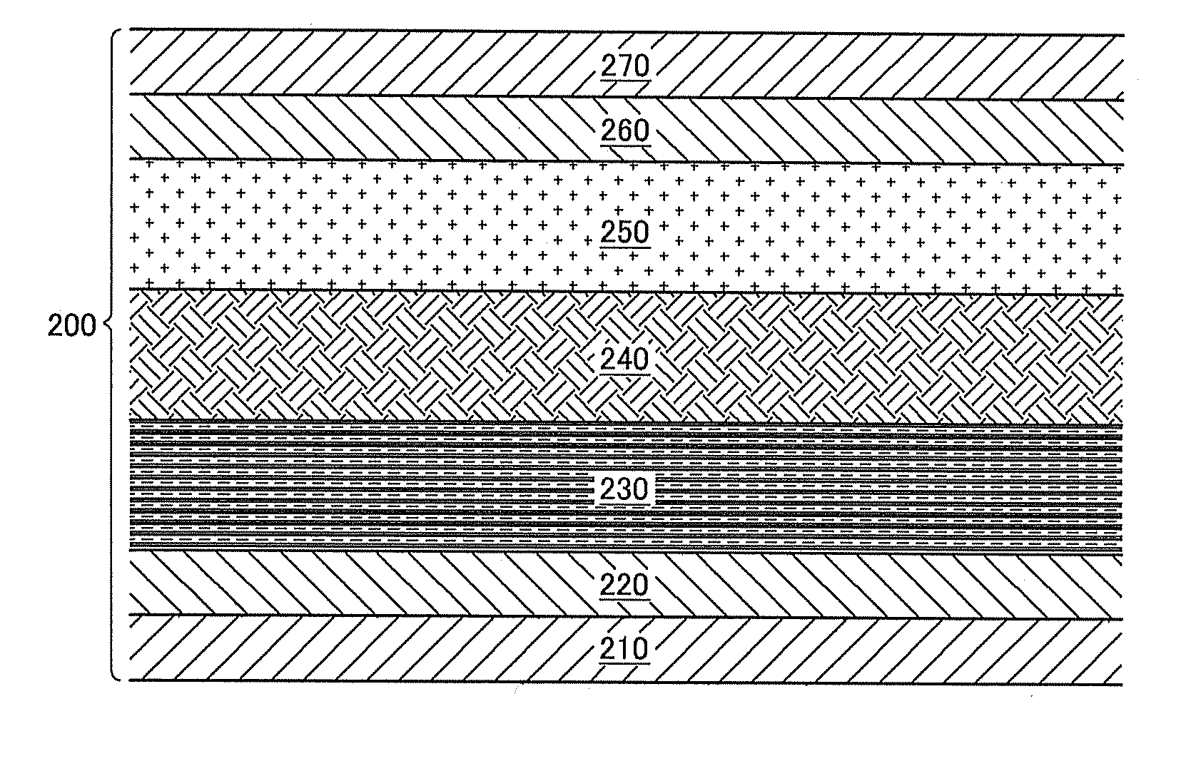
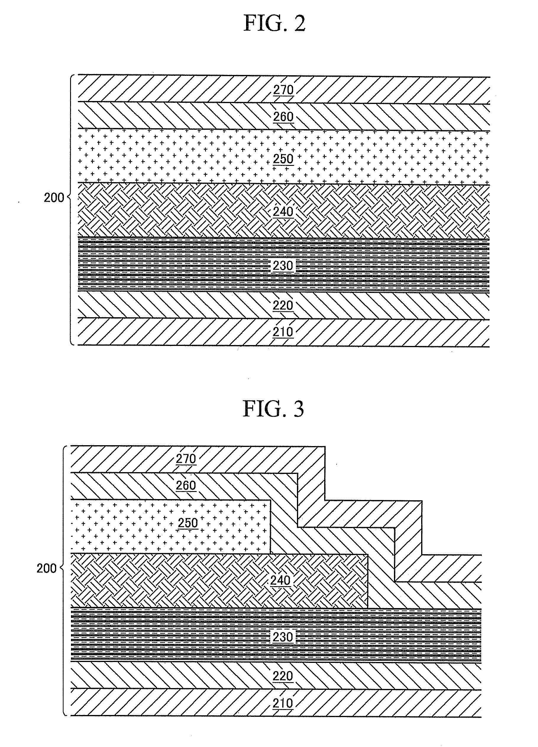
[0009] Accordingly, one aspect of the present invention is to provide an OLED display and a method for manufacturing the same for minimizing interference between organic emission layers.

Problems solved by technology

However, display devices using cathode ray tubes have drawbacks that the volume and weight thereof are large and heavy, respectively, and that they are not easily portable.
Therefore, the liquid crystal display has drawbacks such as high power consumption and slow response speed.
A plasma display device also has drawbacks such as high power consumption, driving complexity and low resolution.
The inherent drawbacks of the plasma display come from the size of the plasma cells necessary to make an individual pixel and the nature of the injected ionizing gas which must be driven therein.
However, the OLED display having different sized pixels has difficulties in design and driving, such as a low response time.
Also, it has difficulties in that its high luminance white light emitting lifespan is reduced because of a strong interaction between the different emission layers.

Method used


Image

  • Organic light emitting diode display
  • Organic light emitting diode display
  • Organic light emitting diode display

Examples


Embodiment Construction

[0018] The present invention now will be described more fully hereinafter with reference to the accompanying drawings, in which exemplary embodiments of the present invention are shown. This invention may, however, be embodied in many different forms and should not be construed as limited to the embodiments set forth herein. Rather, these embodiments are provided so that this disclosure will be thorough and complete, and will fully convey the scope of the invention to those skilled in the art. Like reference numerals refer to like elements throughout.

[0019] It will be understood that when an element is referred to as being “on” another element, it can be directly on the other element or intervening elements may be present therebetween. In contrast, when an element is referred to as being “directly on” another element, there are no intervening elements present. As used herein, the term “and / or” includes any and all combinations of one or more of the associated listed items.

[0020] I...


PUM


Abstract

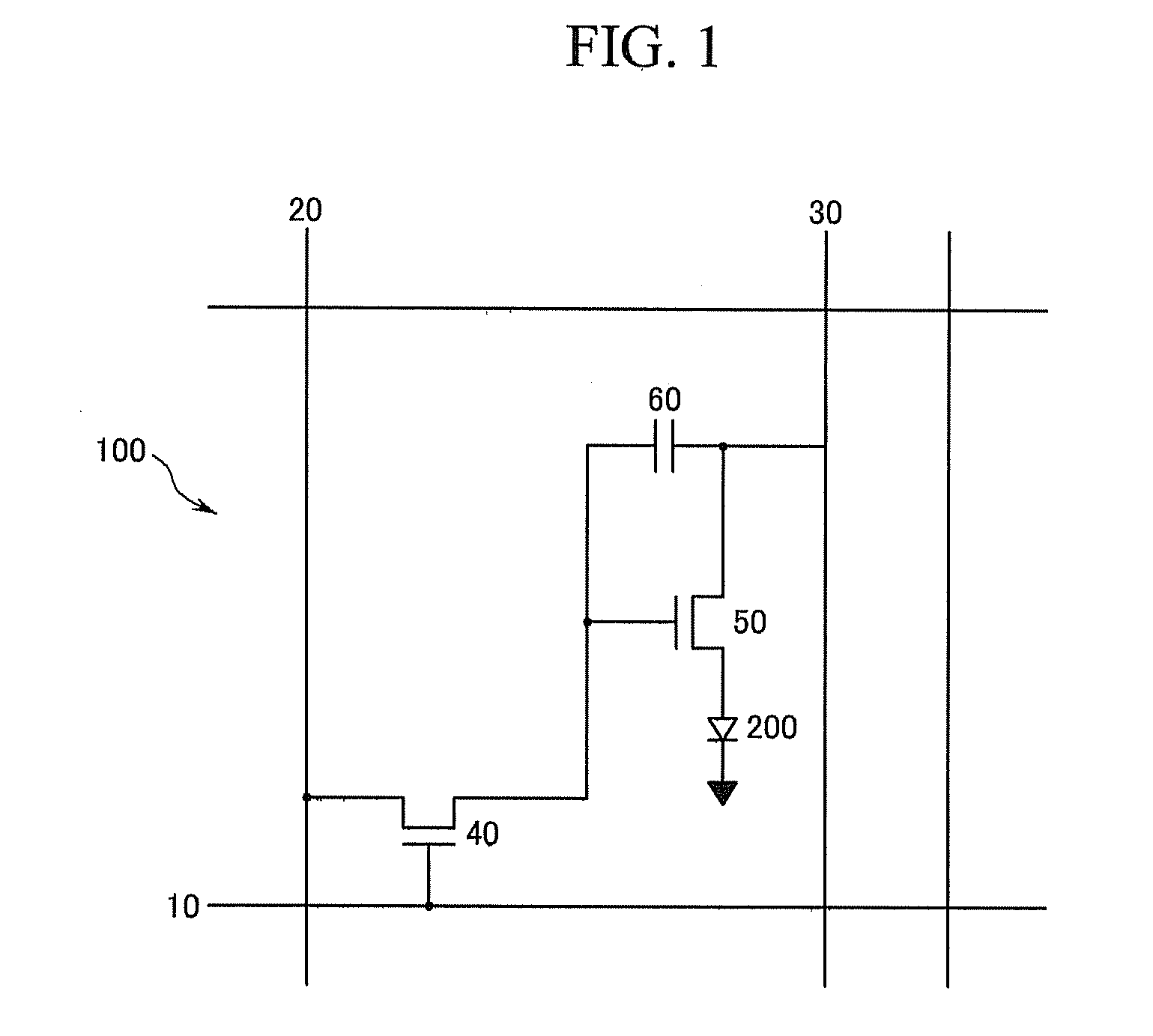
An OLED display for improving white light emitting efficiency and simplifying a manufacturing process includes a plurality of pixels, each of the pixels having a transistor unit, a color filter unit and an organic light emitting device unit. The transistor unit converts signals from the outside into driving signals for driving an organic light emitting device unit. The organic light emitting device unit is composed of blue, red and green emission layers each having different areas. By passing white light through a color filer, the OLED display can realize full color.

Description

[0001] This application claims priority to Korean Patent Application No. 10-2005-0110712, filed on Nov. 18, 2005, and all the benefits accruing therefrom under 35 U.S.C. § 119, the contents of which in its entirety are herein incorporated by reference. BACKGROUND OF THE INVENTION [0002] (a) Field of the Invention [0003] The present invention relates to an organic light emitting diode (“OLED”) display. More particularly, the present invention provides an OLED display and a method of manufacturing the same for improving white light emitting efficiency and simplifying a manufacturing process thereof. [0004] (b) Description of the Related Art [0005] Display devices using a cathode ray tube have been widely used. However, display devices using cathode ray tubes have drawbacks that the volume and weight thereof are large and heavy, respectively, and that they are not easily portable. Recently, in order to overcome the drawbacks of display devices using cathode ray tubes, liquid crystal di...

Claims


Application Information

Patent Timeline
IPC IPC(8): H01J1/62H01J63/04
CPCH01L27/322H01L27/3246H01L51/5036H01L51/56H05B33/14H10K59/38H10K59/122H10K50/125H10K71/00H10K71/60H05B33/10
Inventor SUNG, UN-CHEOLLEE, JOO-HYEON
Owner SAMSUNG DISPLAY CO LTD
Learn More