Electro-optical device, method of manufacturing electro-optical device, and electronic apparatus
- Summary
- Abstract
- Description
- Claims
- Application Information
AI Technical Summary
Benefits of technology
Problems solved by technology
Method used
Image

Examples
first embodiment
[0080] First, an electro-optical device according to a first aspect of the invention, and a method of manufacturing an electro-optical device according to a second aspect of the invention will be described with reference to FIGS. 1 to 12.
Entire Structure of Electro-Optical Device
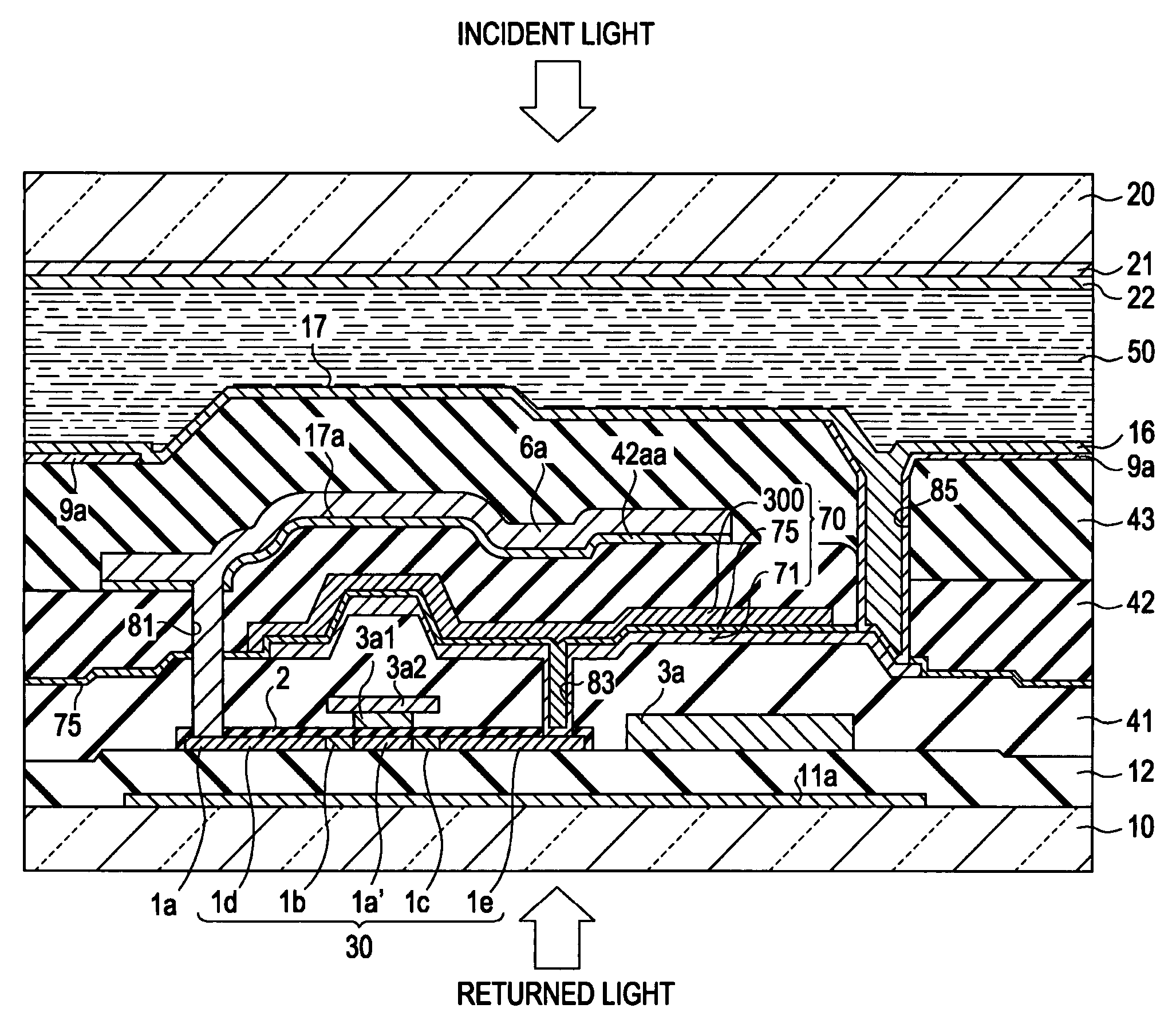
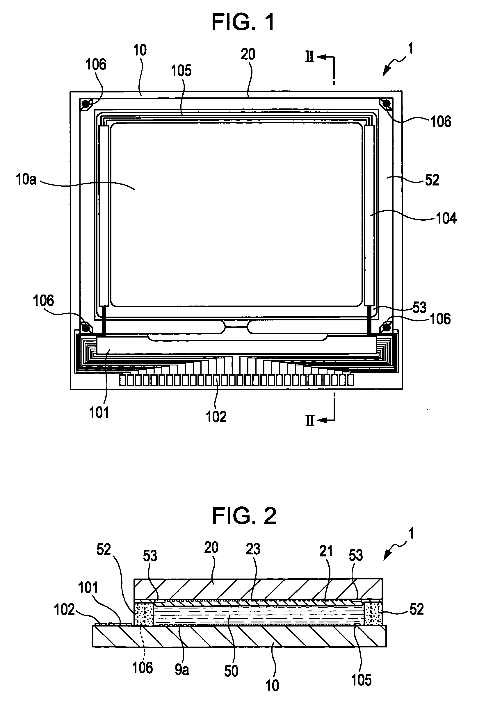
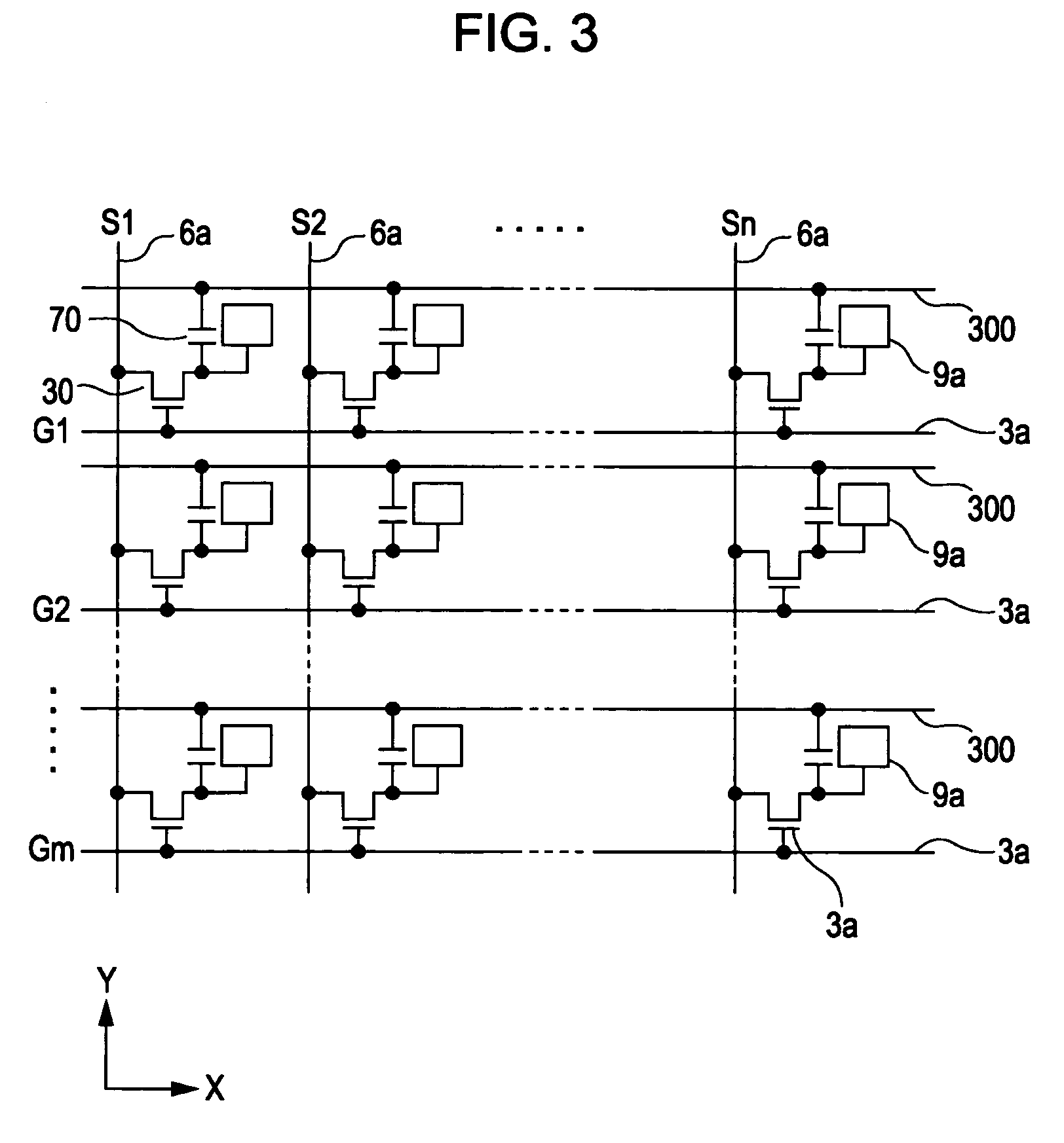
[0081] An electro-optical device according to a first embodiment of the invention will be described with reference to FIGS. 1 and 2. FIG. 1 is a plan view illustrating a TFT array substrate and various essential elements formed on the TFT array substrate in the electro-optical device according to the first embodiment of the invention when viewed from a counter substrate side. FIG. 2 is a cross-sectional view taken along the line of FIG. 1. In this embodiment, as an example of the electro-optical device, a TFT-active-matrix-driven liquid crystal device having a built-in driving circuit will be exemplified.
[0082] In FIGS. 1 and 2, in a liquid crystal device 1, a TFT array substrate 10 is opposite to a coun...
second embodiment
[0147] Next, a method of manufacturing an electro-optical device according to a third aspect of the invention will be described with reference to FIG. 13. In the description below, a process of manufacturing the TFT 30 will be mainly described. In addition, in the description below, the same constituent elements as those in the electro-optical device according to the first embodiment and the method of manufacturing the same are denoted by the same reference numerals, and the description thereof will be omitted.
[0148] In FIG. 13A, in a state in which the channel region 1a′ of the semiconductor layer 1a formed on the TFT array substrate 10 and the impurity region 230 are formed, the conductive film of the second gate electrode 3a2 and the conductive film serving as masks when the impurity region 230 is formed is selectively removed from the side of the conductive film, thereby forming the first gate electrode 3a1.
[0149] Then, as shown in FIG. 13B, the sidewall 91 is formed so as to ...
third embodiment
[0153] Next, an embodiment of a method of manufacturing an electro-optical device according to a fourth aspect of the invention will be described with reference to FIGS. 14 to 16.
[0154] In FIG. 14A, by using the conductive material, such as polysilicon and the like, the first gate electrode 3a1 are formed with the insulating film 2a interposed between the first gate electrode 3a1 and the channel region 1a′ so as to cover the channel region 1a′ in the semiconductor layer 1a formed on the TFT array substrate 10, and impurity ions are doped in the semiconductor layer 1a while using the first gate electrode 3a1 as a mask. Thereby, the impurity region 230 is formed around the channel region 1a′.
[0155] Next, as shown in FIG. 14B, the insulating film 41a made of an insulating material, such as SiO2, is formed so as to cover the impurity region 230 and the first gate electrode 3a1, then the insulating film 41a is polished until the first gate electrode 3a1 is exposed, and the polishing su...
PUM
 Abstract
Description
Claims
Application Information
 - R&D Engineer
- R&D Manager
- IP Professional
- Industry Leading Data Capabilities
- Powerful AI technology
- Patent DNA Extraction
Browse by: Latest US Patents, China's latest patents, Technical Efficacy Thesaurus, Application Domain, Technology Topic.
© 2024 PatSnap. All rights reserved.Legal|Privacy policy|Modern Slavery Act Transparency Statement|Sitemap